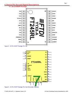
Page 10
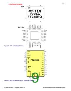
4.4 QFN-32 Package Signal Descriptions
Table 2 - QFN Package Pin Out Description
Pin No. Name
Type Description
USB Interface Group
14
15
USBDP
USBDM
I/O
I/O
USB Data Signal Plus, incorporating internal series resistor and 1.5kΩ pull up resistor to 3.3V
USB Data Signal Minus, incorporating internal series resistor.
Power and Ground Group
1
VCCIO
PWR
+1.8V to +5.25V supply to FIFO Interface and Control group pins (2,3, 6, ...,11, 21, 22, 30,..32). In USB bus
powered designs connect to 3V3OUT to drive out at 3.3V levels, or connect to VCC to drive out at 5V CMOS
level. This pin can also be supplied with an external 1.8V - 2.8V supply in order to drive out at lower levels. It
should be noted that in this case this supply should originate from the same source as the supply to Vcc. This
means that in bus powered designs a regulator which is supplied by the 5V on the USB bus should be used.
4, 17, 20
16
GND
PWR
Device ground supply pins
3V3OUT
Output 3.3V output from integrated L.D.O. regulator. This pin should be decoupled to ground using a 100nF capacitor.
The prime purpose of this pin is to provide the internal 3.3V supply to the USB transceiver cell and the internal
1.5kΩ pull up resistor on USBDP. Up to 50mA can be drawn from this pin to power external logic if required.
This pin can also be used to supply the FT245R’s VCCIO pin.
19
24
VCC
PWR
PWR
3.3V to 5.25V supply to the device core.
AGND
Device analog ground supply for internal clock multiplier
Miscellaneous Signal Group
5, 12, 13, NC
23, 25, 29
NC
No internal connection.
18
RESET#
Input
Can be used by an external device to reset the FT245R. If not required can be left unconnected or pulled up
to VCCIO.
26
27
28
TEST
OSCI
OSCO
Input
Input
Puts the device into I.C. test mode. Must be grounded for normal operation.
Input to 12MHz Oscillator Cell. Optional - Can be left unconnected for normal operation. *
Output Output from 12MHz Oscillator Cell. Optional - Can be left unconnected for normal operation if internal oscilla-
tor is used. *
FIFO Interface and Control Group
30
31
32
D0
D4
D2
I/O
I/O
I/O
FIFO Data Bus Bit 0**
FIFO Data Bus Bit 4**
FIFO Data Bus Bit 2**
2
3
6
7
8
9
D1
I/O
I/O
I/O
I/O
I/O
FIFO Data Bus Bit 1**
FIFO Data Bus Bit 7**
FIFO Data Bus Bit 5**
FIFO Data Bus Bit 6**
FIFO Data Bus Bit 3**
D7
D5
D6
D3
PWREN#
Output Goes low after the device is configured by USB, then high during USB suspend. Can be used to control power
to external logic P-Channel logic level MOSFET switch. Enable the interface pull-down option when using the
PWREN# pin in this way.
10
11
21
RD#
WR
Input
Enables the current FIFO data byte on D0...D7 when low. Fetched the next FIFO data byte (if available) from
the receive FIFO buffer when RD# goes from high to low. See Section 4.5 for timing diagram. **
Input
Writes the data byte on the D0...D7 pins into the transmit FIFO buffer when WR goes from high to low. See
Section 4.5 for timing diagram. **
TXE#
Output When high, do not write data into the FIFO. When low, data can be written into the FIFO by strobing WR high,
then low. During reset this signal pin is tri-state, but pulled up to VCCIO via an internal 200kΩ resistor. See
Section 4.5 for timing diagram.
22
RXF#
Output When high, do not read data from the FIFO. When low, there is data available in the FIFO which can be read
by strobing RD# low, then high again. During reset this signal pin is tri-state, but pulled up to VCCIO via an
internal 200kΩ resistor. See Section 4.5 for timing diagram.
If the Remote Wakeup option is enabled in the internal EEPROM, during USB suspend mode (PWREN# = 1)
RXF# becomes an input which can be used to wake up the host from suspend mode. Strobing the pin low will
cause the device to request a resume on the USB bus.
*Contact FTDI Support for details of how to use an external crystal, ceramic resonator, or oscillator with the FT245R.
** When used in Input Mode, these pins are pulled to VCCIO via internal 200kΩ resistors. These can be programmed
to gently pull low during USB suspend ( PWREN# = “1” ) by setting this option in the internal EEPROM.
FT245R USB UART I.C. Datasheet Version 1.05
© Future Technology Devices International Ltd. 2005

 FTDI [ FUTURE TECHNOLOGY DEVICES INTERNATIONAL LTD. ]