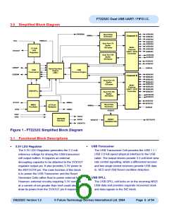
FT2232C Dual USB UART / FIFO I.C.
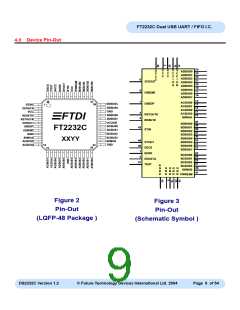
5.0 Pin Definitions
This section decribes the operation of the FT2232C pins. Common pins are defined in the first section, then the I/O
pins are defined, by chip mode. More detailed descriptions of the operation of the I/O pins are provided in section 9.
5.1 Common Pins
The operation of the following FT2232C pins stay the same, regardless of the chip mode :-
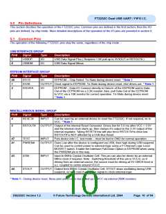
USB INTERFACE GROUP
Pin#
Signal
Type
I/O
Description
7
8
USBDP
USBDM
USB Data Signal Plus ( Requires 1.5K pull-up to 3V3OUT or RSTOUT# )
USB Data Signal Minus
I/O
EEPROM INTERFACE GROUP
Pin#
48
1
Signal
EECS
Type
Description
I/O
EEPROM – Chip Select. Tri-State during device reset. **Note 1
EESK
OUTPUT Clock signal to EEPROM. Tri-State during device reset, else drives out. **Note 1
2
EEDATA
I/O
EEPROM – Data I/O Connect directly to Data-In of the EEPROM and to Data-
Out of the EEPROM via a 2.2K resistor. Also, pull Data-Out of the EEPROM
to VCC via a 10K resistor for correct operation. Tri-State during device reset.
**Note 1
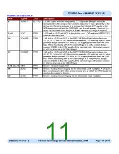
MISCELLANEOUS SIGNAL GROUP
Pin#
4
Signal
Type
Description
RESET#
INPUT
Can be used by an external device to reset the FT2232C. If not required, tie to
VCC. **Note 1
5
RSTOUT#
OUTPUT Output of the internal Reset Generator. Drives low for 5.6 ms after VCC > 3.5V
and the internal clock starts up, then clamps it’s output to the 3.3V output of the
internal regulator. Taking RESET# low will also force RSTOUT# to drive low.
RSTOUT# is NOT affected by a USB Bus Reset.
47
41
TEST
INPUT
Puts device into I.C. test mode – must be tied to GND for normal operation.
PWREN#
OUTPUT Goes Low after the device is configured via USB, then high during USB suspend.
Can be used to control power to external logic using a P-Channel Logic Level
MOSFET switch. Enable the Interface Pull-Down Option in EEPROM when using
the PWREN# pin in this way.
43
44
XTIN
INPUT
Input to 6MHz Crystal Oscillator Cell. This pin can also be driven by an external
6MHz clock if required. Note : Switching threshold of this pin is VCC/2, so if
driving from an external source, the source must be driving at 5V CMOS level or
a.c. coupled to centre around VCC/2.
XTOUT
OUTPUT Output from 6MHz Crystal Oscillator Cell. XTOUT stops oscillating during USB
suspend, so take care if using this signal to clock external logic.
**Note 1 - During device reset, these pins are tri-state but pulled up to VCC via internal 200K resistors.
DS2232C Version 1.2
© Future Technology Devices International Ltd. 2004
Page 10 of 54

 FTDI [ FUTURE TECHNOLOGY DEVICES INTERNATIONAL LTD. ]