FT2232C Dual USB UART / FIFO I.C.
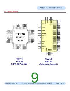
POWER AND GND GROUP
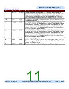
Pin#
6
Signal
Type
Description
3V3OUT
OUTPUT 3.3 volt Output from the integrated L.D.O. regulator This pin should be
decoupled to GND using a 33nF ceramic capacitor in close proximity to the
device pin. It’s prime purpose is to provide the internal 3.3V supply to the
USB transceiver cell and the RSTOUT# pin. A small amount of current (<=
5mA) can be drawn from this pin to power external 3.3V logic if required.
3, 42
14
VCC
PWR
+4.35 volt to +5.25 volt VCC to the device core, LDO and non-UART / FIFO
controller interface pins.
VCCIOA
PWR
+3.0 volt to +5.25 volt VCC to the UART / FIFO A Channel interface pins
10..13, 15..17 and 19..24. When interfacing with 3.3V external logic in a bus
powered design connect VCCIO to a 3.3V supply generated from the USB
bus. When interfacing with 3.3V external logic in a self powered design
connect VCCIO to the 3.3V supply of the external logic. Otherwise connect
to VCC to drive out at 5V CMOS level.
31
VCCIOB
PWR
+3.0 volt to +5.25 volt VCC to the UART / FIFO B Channel interface pins
26..30, 32..33 and 35..40. When interfacing with 3.3V external logic in a bus
powered design connect VCCIO to a 3.3V supply generated from the USB
bus. When interfacing with 3.3V external logic in a self powered design
connect VCCIO to the 3.3V supply of the external logic. Otherwise connect
to VCC to drive out at 5V CMOS level.
9,18, 25, 34 GND
PWR
PWR
Device - Ground Supply Pins
46
AVCC
Device - Analog Power Supply for the internal x8 clock multiplier. A low pass
filter consisting of a 470 Ohm series resistor and a 100 nF to GND should be
used on the supply to this pin.
45
AGND
PWR
Device - Analog Ground Supply for the internal x8 clock multiplier
DS2232C Version 1.2
© Future Technology Devices International Ltd. 2004
Page 11 of 54

 FTDI [ FUTURE TECHNOLOGY DEVICES INTERNATIONAL LTD. ]