FT2232C Dual USB UART / FIFO I.C.
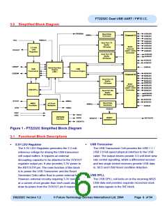
3.0 Simplified Block Diagram
PWREN#
ADBUS0
Baud Rate
Generator
48MHz
Channel A
ADBUS1
ADBUS2
VCC
PWRCTL
ADBUS3
ADBUS4
Dual Port TX
Buffer
128 bytes
ADBUS5
ADBUS6
ADBUS7
Multi-
Purpose
UART / FIFO
Controller
3.3 Volt
LDO
Regulator
3V3OUT
Dual Port RX
Buffer
ACBUS0
ACBUS1
384 Bytes
ACBUS2
ACBUS3
USBDP
USBDM
SI/WUA
Serial Interface
Engine
USB
Transceiver
USB
Protocol Engine
( SIE )
BDBUS0
BDBUS1
BDBUS2
Channel B
Dual Port TX
Buffer
128 bytes
BDBUS3
BDBUS4
Multi-
Purpose
UART / FIFO
Controller
BDBUS5
BDBUS6
BDBUS7
USB DPLL
Dual Port RX
Buffer
384 Bytes
BCBUS0
BCBUS1
BCBUS2
BCBUS3
XTOUT
XTIN
48MHz
12MHz
Baud Rate
Generator
6MHZ
Oscillator
x8 Clock
Multiplier
48MHz
SI/WUB
3V3OUT
TEST
GND
EECS
EESK
EEPROM
Interface
RESET
GENERATOR
RSTOUT#
RESET#
EEDATA
Figure 1 - FT2232C Simplified Block Diagram
3.1 Functional Block Descriptions
•
USB Transceiver
•
3.3V LDO Regulator
The USB Transceiver Cell provides the USB 1.1 /
USB 2.0 full-speed physical interface to the USB
cable. The output drivers provide 3.3 volt level slew
rate control signalling, whilst a differential receiver
and two single ended receivers provide USB data
in, SEO and USB Reset condition detection.
The 3.3V LDO Regulator generates the 3.3 volt
reference voltage for driving the USB transceiver
cell output buffers. It requires an external
decoupling capacitor to be attached to the 3V3OUT
regulator output pin. It also provides 3.3V power to
the RSTOUT# pin. The main function of this block
is to power the USB Transceiver and the Reset
Generator Cells rather than to power external logic.
However, external circuitry requiring 3.3V nominal
at a current of not greater than 5mA could also
draw its power from the 3V3OUT pin if required.
•
USB DPLL
The USB DPLL cell locks on to the incoming NRZI
USB data and provides separate recovered clock
and data signals to the SIE block.
DS2232C Version 1.2
© Future Technology Devices International Ltd. 2004
Page 6 of 54

 FTDI [ FUTURE TECHNOLOGY DEVICES INTERNATIONAL LTD. ]