Freescale Semiconductor, Inc.
During the software-based STOP mode, MCU clocks are stopped, but the MCU con-
tinues to draw power from V . Power supply current is directly proportional to oper-
DD
ating frequency in CMOS integrated circuits and there is very little leakage when the
clocks are stopped. These two factors reduce power consumption while the MCU is in
STOP mode.
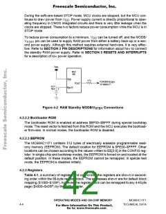
To reduce power consumption to a minimum, V
can be turned off, and the MODB/
DD
V
pin can be used to supply RAM power from either a battery back-up or a sec-
STBY
ond power supply. Although this method requires external hardware, it is very effec-
tive. Refer to SECTION 2 PIN DESCRIPTIONS for information about how to connect
the standby RAM power supply. Refer to SECTION 5 RESETS AND INTERRUPTS
for a description of low power operation.
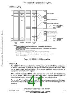
V
DD
MAX
690
V
DD
4.7 k
TO MODB/V
OF M68HC11
STBY
V
OUT
4.8 V
NiCd
V
BATT
+
Figure 4-2 RAM Standby MODB/V
Connections
STBY
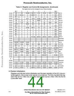
4.2.2.2 Bootloader ROM
The bootloader ROM is enabled at address $BF00–$BFFF during special bootstrap
mode. The reset vector is fetched from this ROM and the MCU executes the bootload-
er firmware. In normal modes, the bootloader ROM is disabled.
4.2.2.3 EEPROM
The MC68HC11F1 contains 512 bytes of electrically erasable programmable read-
only memory (EEPROM). The default location for EEPROM is $FE00–$FFFF. Other
locations can be chosen according to the values written to EE[3:0] in the CONFIG reg-
ister. In single-chip and bootstrap modes, the EEPROM is forced on and located at the
default position. In these modes, the EEPROM cannot be remapped. In special test
mode, the EEPROM is disabled initially.
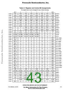
4.2.3 Registers
Table 4-1, a summary of registers and control bits, the registers are shown in ascend-
ing order within the 96-byte register block. The addresses shown are for default block
mapping ($1000–$105F), however, the register block can be remapped to any 4-Kbyte
page ($x000–$x05F) by the INIT register.
OPERATING MODES AND ON-CHIP MEMORY
MC68HC11F1
4-4
TECHNICAL DATA
For More Information On This Product,
Go to: www.freescale.com

 FREESCALE [ Freescale ]