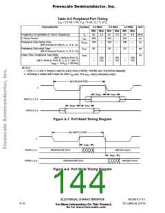
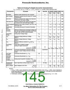
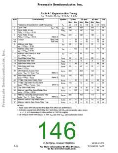
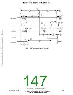
Freescale Semiconductor, Inc.
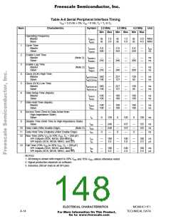
Table A-8 Serial Peripheral Interface Timing
VDD = 5.0 Vdc ± 5%, VSS = 0 Vdc, TA = TL to TH
Num
Characteristic
Symbol
2.0 MHz
3.0 MHz
4.0 MHz
Unit
Min Max Min Max Min Max
Operating Frequency
Master
Slave
f
f
dc
dc
1.0
2.0
dc
dc
1.5
3.0
dc
dc
2.0 MHz
4.0 MHz
op(m)
op(s)
1
2
3
4
5
6
7
8
9
Cycle Time
Master
t
t
2.0
500
—
—
2.0
333
—
—
2.0
250
—
—
t
cyc
ns
cyc(m)
Slave
cyc(s)
Enable Lead Time
Master
(Note 2)
(Note 2)
t
—
250
—
—
—
240
—
—
—
200
—
—
ns
ns
lead(m)
Slave
t
lead(s)
Enable Lag Time
Master
t
t
—
250
—
—
—
240
—
—
—
200
—
—
ns
ns
lag(m)
Slave
lag(s)
Clock (SCK) High Time
Master
Slave
t
t
340
190
—
—
227
127
—
—
130
85
—
—
ns
ns
w(SCKH)m
t
w(SCKH)s
Clock (SCK) Low Time
Master
Slave
340
190
—
—
227
127
—
—
130
85
—
—
ns
ns
w(SCKL)m
t
w(SCKL)s
Data Setup Time (Inputs)
Master
Slave
t
100
100
—
—
100
100
—
—
100
100
—
—
ns
ns
su(m)
t
su(s)
Data Hold Time (Inputs)
Master
Slave
t
100
100
—
—
100
100
—
—
100
100
—
—
ns
ns
h(m)
t
h(s)
Access Time (Time to Data Active from
High-Impedance State)
Slave
t
0
120
0
120
0
120
ns
a
Disable Time (Hold Time to High-Impedance State)
Slave
t
—
—
0
240
240
—
—
—
0
167
167
—
—
—
0
125
125
—
ns
ns
ns
dis
10 Data Valid (After Enable Edge)
11 Data Hold Time (Outputs) (After Enable Edge)
12 Rise Time (20% V to 70% V , C = 200 pF)
(Note 3)
t
v(s)
t
ho
DD
DD
L
SPI Outputs (SCK, MOSI, and MISO)
SPI Inputs (SCK, MOSI, MISO, and SS)
t
t
—
—
100
2.0
—
—
100
2.0
—
—
100
2.0
ns
µs
rm
rs
13 Fall Time (70% V to 20% V , C = 200 pF)
DD
DD
L
SPI Outputs (SCK, MOSI, and MISO)
SPI Inputs (SCK, MOSI, MISO, and SS)
t
t
—
—
100
2.0
—
—
100
2.0
—
—
100
2.0
ns
µs
fm
fs
NOTES:
1. All timing is shown with respect to 20% V and 70% V , unless otherwise noted.
DD
DD
2. Signal production depends on software.
3. Assumes 200 pF load on all SPI pins.
ELECTRICAL CHARACTERISTICS
MC68HC11F1
TECHNICAL DATA
A-14
For More Information On This Product,
Go to: www.freescale.com

 FREESCALE [ Freescale ]