Freescale Semiconductor, Inc.
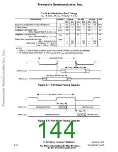
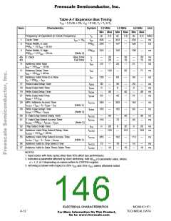
Table A-7 Expansion Bus Timing
VDD = 5.0 Vdc ± 5%, VSS = 0 Vdc, TA = TL to TH
Num
Characteristic
Symbol
2.0 MHz
3.0 MHz
4.0 MHz
Unit
Min Max Min Max Min Max
Frequency of Operation (E-Clock Frequency)
f
dc
2.0
—
dc
3.0
—
dc
4.0 MHz
o
1
2
Cycle Time
t
= 1/f
t
cyc
500
230
333
147
250
105
—
—
ns
ns
cyc
o
Pulse Width, E Low
PW
—
—
EL
PW = 1/2 t – 20 ns
EL
cyc
3
Pulse Width, E High
PW = 1/2 t – 25 ns
PW
225
—
142
—
100
—
ns
EH
(Note 2)
EH
cyc
4A E Clock
4B
Rise Time
FallTime
t
t
—
—
20
20
—
—
20
18
—
—
20
15
ns
ns
r
f
9
Address Hold Time
= 1/8 t – 10 ns
t
t
53
—
103
—
32
—
65
—
82
—
21
—
34
—
71
—
ns
ns
ns
AH
AD
t
AH
cyc
11 Address Delay Time
= 1/8 t + 40 ns
—
t
AD
cyc
12 Address Valid Time to E Rise
= PW – t
t
128
AV
t
AV
EL
AD
17 Read Data Setup Time
18 Read Data Hold Time
19 Write Data Delay Time
21 Write Data Hold Time
t
30
0
—
—
40
—
30
0
—
—
40
—
20
0
—
—
40
—
ns
ns
ns
ns
DSR
t
DHR
t
t
—
63
—
42
—
31
DDW
DHW
t
= 1/8 t
DHW
cyc
29 MPU Address Access Time
= t – t – t – t
AD
t
348
185
—
—
203
102
—
—
144
60
—
—
ns
ns
ACCA
t
(Note 2)
(Note 2)
ACCA
cyc
f
DSR
39 Write Data Setup Time
= PW – t
t
DSW
t
DSW
EH
DDW
50 E Valid Chip Select Delay Time
t
—
40
—
—
40
—
—
40
—
ns
ns
ECSD
51 E Valid Chip Select Access Time
t
155
72
40
ECSA
t
= PW – t
– t
DSR
(Note 2)
(Note 2)
ECSA
EH
ECSD
52 Chip Select Hold Time
54 Address Valid Chip Select Delay Time
= 1/4 t + 40 ns
t
0
20
0
20
0
20
ns
ns
CH
t
—
165
—
123
—
103
ACSD
t
ACSD
cyc
55 Address Valid Chip Select Access Time
= t – t – t – t
t
285
—
162
—
113
—
ns
ACSA
t
ACSA
cyc
f
DSR
ACSD
56 Address Valid to Chip Select Time
t
10
—
—
10
—
—
10
—
—
ns
ns
AVCS
57 Address Valid to Data Three-State Time
t
10
10
10
AVDZ
NOTES:
1. Input clocks with duty cycles other than 50% affect bus performance.
2. Indicates a parameter affected by clock stretching. Add n(t ) to parameter value, where:
cyc
n = 1, 2, or 3 depending on values written to CSSTRH register.
3. All timing is shown with respect to 20% V and 70% V , unless otherwise noted.
DD
DD
ELECTRICAL CHARACTERISTICS
MC68HC11F1
A-12
TECHNICAL DATA
For More Information On This Product,
Go to: www.freescale.com

 FREESCALE [ Freescale ]