Freescale Semiconductor, Inc.
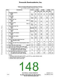
Table A-5 Peripheral Port Timing
VDD = 5.0 Vdc ± 5%, VSS = 0 Vdc, TA = TL to TH
Characteristic
Symbol
2.0 MHz
3.0 MHz
4.0 MHz
Unit
Min Max Min Max Min Max
Frequency of Operation (E-Clock Frequency)
E-Clock Period
f
dc
2.0
—
dc
3.0
—
dc
4.0 MHz
o
t
500
100
333
100
250
100
—
—
ns
ns
cyc
Peripheral Data Setup Time
t
—
—
PDSU
(MCU Read of Ports A, C, D, E, G)
Peripheral Data Hold Time
t
50
—
50
—
50
—
ns
ns
PDH
(MCU Read of Ports A, C, D, E, G)
Delay Time, Peripheral Data Write
(MCU Write to Port A)
t
PWD
—
—
200
225
—
—
200
183
—
—
200
162
(MCU Write to Ports B, C, D, F, and G
t
= 1/4 t + 100 ns)
PWD
cyc
NOTES:
1. Ports C, D, and G timing is valid for active drive (CWOM, DWOM, and GWOM bits cleared).
2. All timing is shown with respect to 20% V and 70% V , unless otherwise noted.
DD
DD
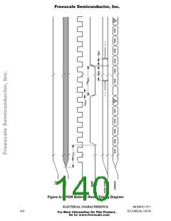
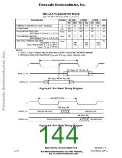
MCU READ OF PORT
E
PORTS A, C, D, F
PORTS B, E, G
t
t
PDH
PDSU
t
t
PDH
PDSU
Figure A-7 Port Read Timing Diagram
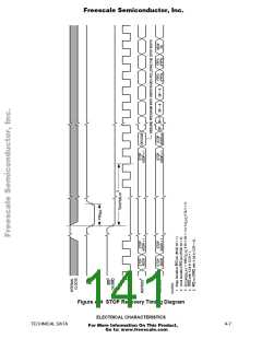
MCU WRITE TO PORT
E
t
PWD
PORTS C, D, F
PORTS A, B, G
PREVIOUS PORT DATA
NEW DATA VALID
t
PWD
PREVIOUS PORT DATA
NEW DATA VALID
Figure A-8 Port Write Timing Diagram
ELECTRICAL CHARACTERISTICS
MC68HC11F1
A-10
TECHNICAL DATA
For More Information On This Product,
Go to: www.freescale.com

 FREESCALE [ Freescale ]