Freescale Semiconductor, Inc.
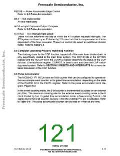
PAOVI
1
PAOVF
INTERRUPT
REQUESTS
PAII
2
PAIF
E ÷ 64 CLOCK
(FROM MAIN TIMER)
P
P
P
P AI
TMSK2 INT ENABLES
TFLG2 INTERRUPT STATUS
PAI EDGE
PAEN
DISABLE
FLAG SETTING
OVERFLOW
PACNT 8-BIT COUNTER
ENABLE
PIN
2:1
MUX
CLOCK
PAEN
PA7/
PAI/
OC1
INPUT BUFFER
AND
EDGE DETECTOR
DATA BUS
OUTPUT
BUFFER
FROM
MAIN TIMER
OC1
FROM DATA
DIRECTION
BIT FOR
PACTL CONTROL
PORT A PIN 7
INTERNAL
DATA BUS
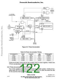
Figure 9-3 Pulse Accumulator
Table 9-5 Pulse Accumulator Timing
6
Crystal Frequency
E Clock
(E)
Cycle Time
(1/E)
2 /E
PACNT Overflow
(4 E)
(64/E)
(16384/E)
16.384 ms
8.192 ms
5.461 ms
4.096 ms
4.0 MHz
8.0 MHz
12.0 MHz
16.0 MHz
1.0 MHz
2.0 MHz
3.0 MHz
4.0 MHz
1000 ns
500 ns
333 ns
250 ns
64 µs
32 µs
21.33 µs
16.0 µs
Pulse accumulator control bits are also located within two timer registers, TMSK2 and
TFLG2, as described in the following paragraphs.
9.6.1 Pulse Accumulator Control Register
Four of this register's bits control an 8-bit pulse accumulator system. Another bit en-
ables either the OC5 function or the IC4 function, while two other bits select the rate
for the real-time interrupt system.
TIMING SYSTEM
MC68HC11F1
9-16
TECHNICAL DATA
For More Information On This Product,
Go to: www.freescale.com

 FREESCALE [ Freescale ]