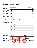
Detailed Register Address Map
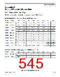
0x0020-0x002F Debug Module (S12SDBG) Map
Address
Name
Bit 7
Bit 6
Bit 5
Bit 4
Bit 3
Bit 2
Bit 1
Bit 0
R
W
R
0
0
0
0x0028
DBGCCTL
TAG
0
BRK
0
RW
0
RWE
0
COMPE
(3)
0
0
0x0029
0x002A
0x002B
0x002C
0x002D
0x002E
0x002F
DBGXAH
DBGXAM
DBGXAL
17
9
Bit 16
Bit 8
Bit 0
Bit 8
Bit 0
Bit 8
Bit 0
W
R
Bit 15
Bit 7
14
6
13
5
12
4
11
3
10
2
W
R
1
W
R
DBGADH
DBGADL
DBGADHM
DBGADLM
Bit 15
Bit 7
14
6
13
5
12
4
11
3
10
2
9
W
R
1
W
R
Bit 15
Bit 7
14
6
13
5
12
4
11
3
10
2
9
W
R
1
W
1. This represents the contents if the Comparator A or C control register is blended into this address
2. This represents the contents if the Comparator B or D control register is blended into this address
3. This represents the contents if the Comparator B or D control register is blended into this address
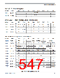
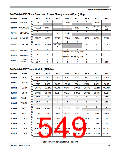
0x0030-0x0033 Reserved
Address
Name
Bit 7
Bit 6
Bit 5
Bit 4
Bit 3
Bit 2
Bit 1
Bit 0
R
W
R
0
0
0
0
0
0
0
0
0x0030
Reserved
0
0
0
0
0
0
0
0
0
0
0
0
0
0
0
0
0
0
0
0
0
0
0
0
0x0031
0x0032
0x0033
Reserved
Reserved
Reserved
W
R
W
R
W
0x0034-0x003F Clock Reset and Power Management (CPMU) Map
Address
Name
Bit 7
VCOFRQ[1:0]
REFFRQ[1:0]
Bit 6
Bit 5
Bit 4
Bit 3
Bit 2
Bit 1
Bit 0
R
W
R
0x0034 CPMUSYNR
0x0035 CPMUREFDIV
SYNDIV[5:0]
REFDIV[3:0]
0
0
0
W
R
0
0
CPMUPOSTDI
0x0036
V
POSTDIV[4:0]
ILAF
W
R
LOCK
UPOSC
0x0037
CPMUFLG
RTIF
PORF
LVRF
LOCKIF
OSCIF
W
S12P-Family Reference Manual, Rev. 1.13
548
Freescale Semiconductor

 FREESCALE [ Freescale ]