Detailed Register Address Map
Appendix D
Detailed Register Address Map
D.1
Detailed Register Map
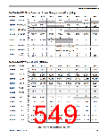
The following tables show the detailed register map of the MC9S12P-Family.
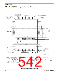
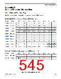
0x0000-0x0009 Port Integration Module (PIM) Map 1 of 4
Address
Name
Bit 7
Bit 6
Bit 5
Bit 4
Bit 3
Bit 2
Bit 1
Bit 0
R
W
R
0x0000
PORTA
PA7
PA6
PA5
PA4
PA3
PA2
PA1
PA0
0x0001
0x0002
0x0003
0x0004
0x0005
0x0006
0x0007
0x0008
0x0009
PORTB
DDRA
PB7
PB6
PB5
PB4
PB3
PB2
PB1
PB0
W
R
DDRA7
DDRA6
DDRA5
DDRA4
DDRA3
DDRA2
DDRA1
DDRA0
W
R
DDRB
DDRB7
0
DDRB6
0
DDRB5
0
DDRB4
0
DDRB3
0
DDRB2
0
DDRB1
0
DDRB0
0
W
R
Reserved
Reserved
Reserved
Reserved
PORTE
DDRE
W
R
0
0
0
0
0
0
0
0
0
0
0
0
0
0
0
0
0
0
0
0
0
0
W
R
W
R
0
0
W
R
PE1
0
PE0
0
PE7
PE6
PE5
PE4
PE3
PE2
W
R
DDRE7
DDRE6
DDRE5
DDRE4
DDRE3
DDRE2
W
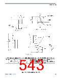
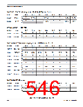
0x000A-0x000B Module Mapping Conrol (MMC) Map 1 of 2
Address
Name
Bit 7
Bit 6
Bit 5
Bit 4
Bit 3
Bit 2
Bit 1
Bit 0
R
W
R
0
0
0
0
0
0
0
0
0x000A
Reserved
0
0
0
0
0
0
0
0x000B
MODE
MODC
W
S12P-Family Reference Manual, Rev. 1.13
Freescale Semiconductor
545

 FREESCALE [ Freescale ]