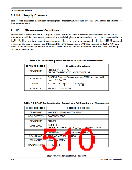
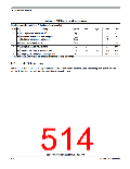
Electrical Characteristics
Table A-15. ATD Electrical Characteristics
Conditions are shown in Table A-4 unless otherwise noted
Num
C
Rating
Symbol
Min
Typ
Max
Unit
1
2
C Max input source resistance(1)
RS
—
—
1
KΩ
D Total input capacitance Non sampling
Total input capacitance Sampling
CINN
CINS
—
—
—
—
10
16
pF
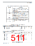
RINA
3
4
5
6
D Input internal Resistance
-
5
15
kΩ
mA
A/A
A/A
C Disruptive analog input current
C Coupling ratio positive current injection
C Coupling ratio negative current injection
INA
Kp
Kn
-2.5
—
—
—
—
2.5
1E-4
5E-3
—
1. 1 Refer to A.2.2.2 for further information concerning source resistance
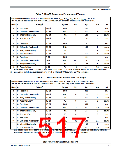
A.2.3
ATD Accuracy
Table A-16. and Table A-17. specifies the ATD conversion performance excluding any errors due to
current injection, input capacitance and source resistance.
S12P-Family Reference Manual, Rev. 1.13
514
Freescale Semiconductor

 FREESCALE [ Freescale ]