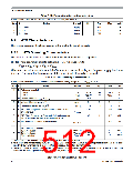
Electrical Characteristics
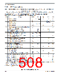
Table A-13. Pseudo Stop Current Characteristics
Conditions are: VDDR=5.5V, RTI and COP and API enabled, see Table A-8.
Num
C
Rating
Symbol
Min
Typ
Max
Unit
1
2
3
C
C
C
150°C
-40°C
25°C
IDDPS
IDDPS
IDDPS
450
175
200
µA
µA
µA
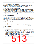
A.2
ATD Characteristics
This section describes the characteristics of the analog-to-digital converter.
A.2.1
ATD Operating Characteristics
The Table A-14 and Table A-15 show conditions under which the ATD operates.
The following constraints exist to obtain full-scale, full range results:
V
≤ V ≤ V ≤ V ≤ V
.
DDA
SSA
RL
IN
RH
This constraint exists since the sample buffer amplifier can not drive beyond the power supply levels that
it ties to. If the input level goes outside of this range it will effectively be clipped.
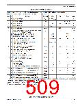
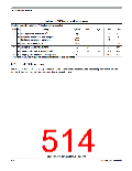
Table A-14. ATD Operating Characteristics
Conditions are shown in Table A-4 unless otherwise noted, supply voltage 3.13 V < VDDA < 5.5 V
Num
C
Rating
Symbol
Min
Typ
Max
Unit
1
D Reference potential
Low
High
VRL
VRH
VSSA
VDDA/2
—
—
VDDA/2
VDDA
V
V
2
3
4
5
D Voltage difference VDDX to VDDA
D Voltage difference VSSX to VSSA
C Differential reference voltage(1)
∆
–2.35
–0.1
3.13
0.25
0
0
0.1
0.1
5.5
8.0
V
V
VDDX
∆
VSSX
VRH-VRL
5.0
V
C ATD Clock Frequency (derived from bus clock via the
prescaler bus)
MHz
fATDCLk
6
7
P ATD Clock Frequency in Stop mode (internal generated
temperature and voltage dependent clock, ICLK)
0.6
—
1
1.7
1.5
MHz
us
D ADC conversion in stop, recovery time(2)
tATDSTPRC
—
V
ATD Conversion Period(3)
12 bit resolution:
10 bit resolution:
8 bit resolution:
NCONV12
NCONV10
NCONV8
20
19
17
42
41
39
ATD
clock
Cycles
8
D
1. Full accuracy is not guaranteed when differential voltage is less than 4.50 V
2. When converting in Stop Mode (ICLKSTP=1) an ATD Stop Recovery time tATDSTPRCV is required to switch back to bus clock
based ATDCLK when leaving Stop Mode. Do not access ATD registers during this time.
3. The minimum time assumes a sample time of 4 ATD clock cycles. The maximum time assumes a sample time of 24 ATD clock
cycles and the discharge feature (SMP_DIS) enabled, which adds 2 ATD clock cycles.
S12P-Family Reference Manual, Rev. 1.13
512
Freescale Semiconductor

 FREESCALE [ Freescale ]