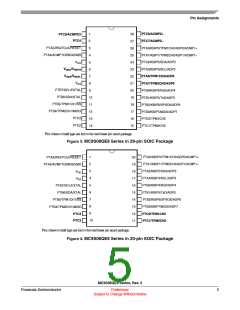
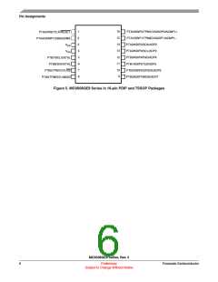
Electrical Characteristics
Input must be current limited to the value specified. To determine the value of the required
1
current-limiting resistor, calculate resistance values for positive (VDD) and negative (VSS) clamp
voltages, then use the larger of the two resistance values.
2
3
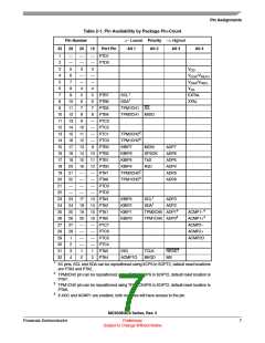
All functional non-supply pins, except for PTA5 are internally clamped to VSS and VDD
.
Power supply must maintain regulation within operating VDD range during instantaneous and
operating maximum current conditions. If positive injection current (VIn > VDD) is greater than
IDD, the injection current may flow out of VDD and could result in external power supply going
out of regulation. Ensure external VDD load will shunt current greater than maximum injection
current. This will be the greatest risk when the MCU is not consuming power. Examples are: if
no system clock is present, or if the clock rate is very low (which would reduce overall power
consumption).
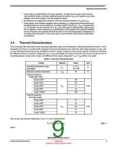
3.4
Thermal Characteristics
This section provides information about operating temperature range, power dissipation, and package thermal resistance. Power
dissipation on I/O pins is usually small compared to the power dissipation in on-chip logic and voltage regulator circuits, and
it is user-determined rather than being controlled by the MCU design. To take P into account in power calculations, determine
I/O
the difference between actual pin voltage and V or V and multiply by the pin current for each I/O pin. Except in cases of
SS
DD
unusually high pin current (heavy loads), the difference between pin voltage and V or V will be very small.
SS
DD
Table 4. Thermal Characteristics
Symbol
Rating
Value
Unit
Operating temperature range
(packaged)
TL to TH
–40 to 85
TA
°C
°C
Maximum junction temperature
TJM
95
Thermal resistance
Single-layer board
32-pin LQFP
28-pin SOIC
20-pin SOIC
16-pin PDIP
16-pin TSSOP
66
57
θJA
71
°C/W
64
108
Thermal resistance
Four-layer board
32-pin LQFP
28-pin SOIC
20-pin SOIC
16-pin PDIP
16-pin TSSOP
47
42
52
47
78
θJA
°C/W
The average chip-junction temperature (T ) in °C can be obtained from:
J
T = T + (P × θ )
JA
Eqn. 1
J
A
D
where:
MC9S08QE8 Series, Rev. 3
Freescale Semiconductor
Preliminary
9
Subject to Change Without Notice

 FREESCALE [ Freescale ]