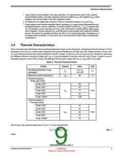
Electrical Characteristics
T = Ambient temperature, °C
A
θ
= Package thermal resistance, junction-to-ambient, °C/W
JA
P = P + P
D
int
I/O
P
P
= I × V , Watts — chip internal power
= Power dissipation on input and output pins — user determined
int
I/O
DD DD
For most applications, P << P and can be neglected. An approximate relationship between P and T (if P is neglected)
I/O
int
D
J
I/O
is:
P = K ÷ (T + 273°C)
Eqn. 2
D
J
Solving Equation 1 and Equation 2 for K gives:
K = P × (T + 273°C) + θ × (P )
2
Eqn. 3
D
A
JA
D
where K is a constant pertaining to the particular part. K can be determined from equation 3 by measuring P (at equilibrium)
D
for a known T . Using this value of K, the values of P and T can be obtained by solving Equation 1 and Equation 2 iteratively
A
D
J
for any value of T .
A
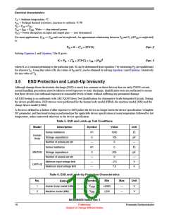
3.5
ESD Protection and Latch-Up Immunity
Although damage from electrostatic discharge (ESD) is much less common on these devices than on early CMOS circuits,
normal handling precautions must be taken to avoid exposure to static discharge. Qualification tests are performed to ensure
that these devices can withstand exposure to reasonable levels of static without suffering any permanent damage.
All ESD testing is in conformity with AEC-Q100 Stress Test Qualification for Automotive Grade Integrated Circuits. During
the device qualification, ESD stresses were performed for the human body model (HBM), the machine model (MM) and the
charge device model (CDM).
A device is defined as a failure if after exposure to ESD pulses the device no longer meets the device specification. Complete
DC parametric and functional testing is performed per the applicable device specification at room temperature followed by hot
temperature, unless instructed otherwise in the device specification.
Table 5. ESD and Latch-up Test Conditions
Model
Description
Series resistance
Symbol
Value
Unit
R1
1500
Ω
pF
—
Human
Body
Storage capacitance
C
100
3
Number of pulses per pin
—
Series resistance
R1
0
Ω
pF
—
V
Machine
Latch-up
Storage capacitance
C
200
3
Number of pulses per pin
Minimum input voltage limit
Maximum input voltage limit
—
—
—
–2.5
7.5
V
Table 6. ESD and Latch-Up Protection Characteristics
1
No.
1
Symbol
VHBM
Min
±2000
±200
Max
—
Unit
V
Rating
Human body model (HBM)
Machine model (MM)
VMM
2
—
V
MC9S08QE8 Series, Rev. 3
10
Preliminary
Freescale Semiconductor
Subject to Change Without Notice

 FREESCALE [ Freescale ]