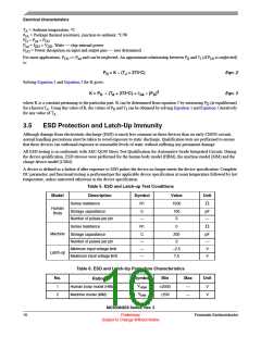
Electrical Characteristics
Table 6. ESD and Latch-Up Protection Characteristics (continued)
VCDM
ILAT
3
4
Charge device model (CDM)
±500
±100
—
—
V
Latch-up current at TA = 85°C
mA
1
Parameter is achieved by design characterization on a small sample size from typical devices
under typical conditions unless otherwise noted.
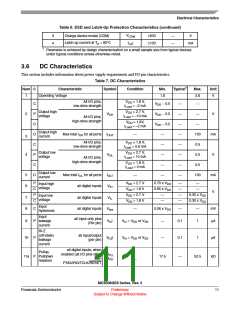
3.6
DC Characteristics
This section includes information about power supply requirements and I/O pin characteristics.
Table 7. DC Characteristics
Num C
Characteristic
Symbol
Condition
Min.
Typical1
Max.
Unit
1
Operating Voltage
1.8
3.6
V
All I/O pins,
low-drive strength
VDD > 1.8 V,
ILoad = –2 mA
C
VDD – 0.5
VDD – 0.5
—
—
—
—
—
—
—
—
—
—
Output high
voltage
VDD > 2.7 V,
ILoad = –10 mA
2
P
C
D
C
P
C
D
VOH
V
mA
V
All I/O pins,
high-drive strength
VDD > 1.8V,
ILoad = –2 mA
VDD – 0.5
—
Output high
current
Max total IOH for all ports IOHT
—
—
—
—
—
—
100
0.5
0.5
0.5
100
3
4
All I/O pins,
low-drive strength
VDD > 1.8 V,
ILoad = 0.6 mA
Output low
voltage
VDD > 2.7 V,
ILoad = 10 mA
VOL
All I/O pins,
high-drive strength
VDD > 1.8 V,
ILoad = 3 mA
Output low
current
5
6
Max total IOL for all ports
all digital inputs
IOLT
VIH
—
mA
V
P
C
P
C
VDD > 2.7 V
VDD > 1.8 V
VDD > 2.7 V
VDD > 1.8 V
0.70 x VDD
—
—
—
—
—
Input high
voltage
0.85 x VDD
—
—
—
0.35 x VDD
0.30 x VDD
Input low
voltage
7
8
all digital inputs
VIL
Input
hysteresis
C
all digital inputs Vhys
—
0.06 x VDD
—
—
mV
Input
P leakage
current
all input only pins
|IIn|
9
VIn = VDD or VSS
—
0.1
1
μA
(Per pin)
Hi-Z
(off-state)
leakage
current
all input/output
10
P
|IOZ
|
VIn = VDD or VSS
—
0.1
—
1
μA
kΩ
(per pin)
all digital inputs, when
enabled (all I/O pins other RPU,
Pullup,
11a P Pulldown
resistors
17.5
52.5
than
RPD
—
PTA5/IRQ/TCLK/RESET
MC9S08QE8 Series, Rev. 3
Freescale Semiconductor
Preliminary
11
Subject to Change Without Notice

 FREESCALE [ Freescale ]