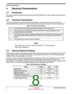
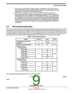
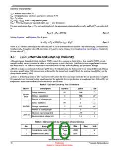
Electrical Characteristics
Table 7. DC Characteristics (continued)
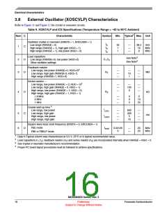
Num C
Characteristic
Symbol
Condition
Min.
Typical1
Max.
Unit
RPU,
RPD
Pullup,
11b C Pulldown
resistors
(PTA5/IRQ/TCLK/RESET)
Single pin limit
—
17.5
—
52.5
kΩ
(Note2)
–0.2
–5
—
—
0.2
5
mA
mA
DCinjection
12 C current 3, 4,
IIC
VIN < VSS, VIN > VDD
Total MCU limit, includes
sum of all stressed pins
5
13 C Input Capacitance, all pins
14 C RAM retention voltage
15 C POR re-arm voltage6
16 D POR re-arm time
CIn
—
—
—
—
—
—
—
0.6
1.4
—
8
pF
V
VRAM
VPOR
tPOR
1.0
2.0
—
0.9
10
V
μs
VDD falling
VDD rising
1.80
1.88
1.84
1.92
1.88
1.96
17 P Low-voltage detection threshold
VLVD
VLVW
V
V
VDD falling
VDD rising
18 P Low-voltage warning threshold
Low-voltage inhibit reset/recover
2.08
2.14
2.24
19
P
Vhys
VBG
—
—
—
80
—
mV
V
hysteresis
20 P Bandgap Voltage Reference7
1.15
1.17
1.18
1
2
Typical values are measured at 25°C. Characterized, not tested
The specified resistor value is the actual value internal to the device. The pullup or pulldown value may appear higher when
measured externally on the pin.
3
4
All functional non-supply pins, except for PTA5 are internally clamped to VSS and VDD
.
Input must be current limited to the value specified. To determine the value of the required current-limiting resistor, calculate
resistance values for positive and negative clamp voltages, then use the larger of the two values.
5
Power supply must maintain regulation within operating VDD range during instantaneous and operating maximum current
conditions. If the positive injection current (VIn > VDD) is greater than IDD, the injection current may flow out of VDD and could
result in external power supply going out of regulation. Ensure that external VDD load will shunt current greater than maximum
injection current. This will be the greatest risk when the MCU is not consuming power. Examples are: if no system clock is
present, or if clock rate is very low (which would reduce overall power consumption).
6
7
Maximum is highest voltage that POR is guaranteed.
Factory trimmed at VDD = 3.0 V, Temp = 25 °C
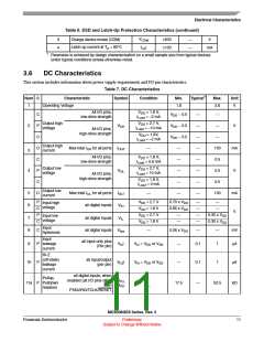
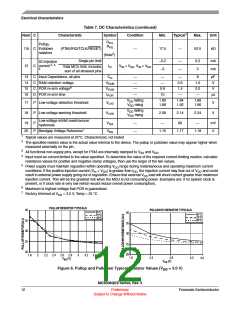
PULLUP RESISTOR TYPICALS
PULLDOWN RESISTOR TYPICALS
40
35
30
25
20
85°C
40
35
30
25
20
85°C
25°C
25°C
–40°C
–40°C
1.8
2
2.2 2.4 2.6 2.8
3
3.2 3.4 3.6
1.8
2.3
2.8
VDD (V)
3.3
3.6
VDD (V)
Figure 6. Pullup and Pulldown Typical Resistor Values (V = 3.0 V)
DD
MC9S08QE8 Series, Rev. 3
12
Preliminary
Freescale Semiconductor
Subject to Change Without Notice

 FREESCALE [ Freescale ]