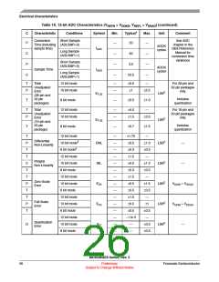
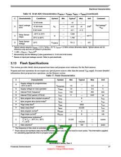
Electrical Characteristics
Table 14. Analog Comparator Electrical Specifications (continued)
C
Characteristic
Analog input voltage
Symbol
Min
Typical
Max
Unit
D
P
C
VAIN
VAIO
VH
VSS – 0.3
—
20
VDD
40
V
Analog input offset voltage
—
mV
mV
Analog comparator hysteresis
3.0
9.0
15.0
IALKG
tAINIT
P
C
Analog input leakage current
—
—
—
—
1.0
1.0
μA
μs
Analog comparator initialization delay
3.12 ADC Characteristics
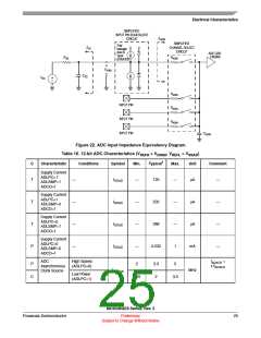
Table 15. 12-bit ADC Operating Conditions
Characteristic
Conditions
Symb
Min
Typ1
Max
Unit
Comment
Supply voltage
Absolute
Delta to VDD (VDD-VDDAD
VDDAD
ΔVDDAD
ΔVSSAD
1.8
—
0
3.6
V
—
—
—
2
)
–100
–100
+100
+100
mV
mV
2
Ground voltage
Delta to VSS (VSS-VSSAD
)
0
Ref Voltage
High
—
—
—
VREFH
VADIN
CADIN
1.8
VREFL
—
VDDAD
—
VDDAD
VREFH
5.5
V
V
—
—
—
Input Voltage
Input
Capacitance
4.5
pF
Input
Resistance
—
RADIN
—
5
7
kΩ
kΩ
—
Analog Source
Resistance
12 bit mode
fADCK > 4MHz
fADCK < 4MHz
—
—
—
—
2
5
10 bit mode
RAS
External to MCU
f
ADCK > 4MHz
—
—
—
—
5
10
fADCK < 4MHz
8 bit mode (all valid fADCK
High Speed (ADLPC=0)
Low Power (ADLPC=1)
)
—
—
—
10
ADC
Conversion
Clock Freq.
0.4
8.0
fADCK
MHz
—
0.4
—
4.0
1
2
Typical values assume VDDAD = 3.0 V, Temp = 25 °C, fADCK=1.0 MHz unless otherwise stated. Typical values are for
reference only and are not tested in production.
DC potential difference.
MC9S08QE8 Series, Rev. 3
24
Preliminary
Freescale Semiconductor
Subject to Change Without Notice

 FREESCALE [ Freescale ]