Electrical Characteristics
3.10.1 Control Timing
Table 11. Control Timing
Num
C
D
D
D
D
Rating
Symbol
fBus
tLPO
textrst
trstdrv
Min
Typical1
Max
10
Unit
MHz
μs
Bus frequency (tcyc = 1/fBus
)
1
2
3
4
dc
700
—
—
—
—
Internal low power oscillator period
1300
—
External reset pulse width2
Reset low drive
100
ns
34 x tcyc
—
ns
BKGD/MS setup time after issuing background debug
force reset to enter user or BDM modes
tMSSU
tMSH
5
6
D
D
500
100
—
—
—
—
ns
BKGD/MS hold time after issuing background debug
force reset to enter user or BDM modes 3
μs
IRQ pulse width
Asynchronous path2
Synchronous path4
tILIH, IHIL
t
100
1.5 × tcyc
—
—
—
—
ns
ns
7
D
8
D
Keyboard interrupt pulse width
Asynchronous path2
tILIH, IHIL
t
100
1.5 × tcyc
—
—
—
—
Synchronous path4
Port rise and fall time —
Low output drive (PTxDS = 0) (load = 50 pF)5
Slew rate control disabled (PTxSE = 0)
Slew rate control enabled (PTxSE = 1)
t
Rise, tFall
ns
ns
—
—
16
23
—
—
9
C
Port rise and fall time —
High output drive (PTxDS = 1) (load = 50 pF)5
Slew rate control disabled (PTxSE = 0)
Slew rate control enabled (PTxSE = 1)
tRise, tFall
—
—
5
9
—
—
1
2
3
Typical values are based on characterization data at VDD = 3.0V, 25°C unless otherwise stated.
This is the shortest pulse that is guaranteed to be recognized as a reset pin request.
To enter BDM mode following a POR, BKGD/MS should be held low during the power-up and for a hold time of tMSH after VDD
rises above VLVD
.
4
5
This is the minimum pulse width that is guaranteed to pass through the pin synchronization circuitry. Shorter pulses may or
may not be recognized. In stop mode, the synchronizer is bypassed so shorter pulses can be recognized.
Timing is shown with respect to 20% VDD and 80% VDD levels. Temperature range –40°C to 85°C.
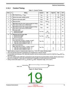
textrst
RESET PIN
Figure 14. Reset Timing
MC9S08QE8 Series, Rev. 3
Freescale Semiconductor
Preliminary
19
Subject to Change Without Notice

 FREESCALE [ Freescale ]