Electrical Characteristics
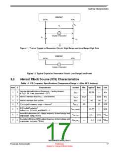
Table 10. ICS Frequency Specifications (Temperature Range = –40 to 85°C Ambient) (continued)
Num
C
Characteristic
Symbol
Min. Typical1 Max.
Unit
Total deviation of trimmed DCO output frequency over voltage
and temperature
+ 0.5
Δfdco_t
%fdco
8
C
—
± 2
-1.0
± 0.5
—
Total deviation of trimmed DCO output frequency over fixed
voltage and temperature range of 0°C to 70 °C
Δfdco_t
tAcquire
CJitter
%fdco
ms
9
C
C
C
—
—
—
± 1
1
FLL acquisition time3
10
11
Long term jitter of DCO output clock (averaged over 2-ms
interval)4
%fdco
0.02
0.2
1
2
3
Data in Typical column was characterized at 3.0 V, 25°C or is typical recommended value.
The resulting bus clock frequency should not exceed the maximum specified bus clock frequency of the device.
This specification applies to any time the FLL reference source or reference divider is changed, trim value changed or changing
from FLL disabled (FBELP, FBILP) to FLL enabled (FEI, FEE, FBE, FBI). If a crystal/resonator is being used as the reference,
this specification assumes it is already running.
4
Jitter is the average deviation from the programmed frequency measured over the specified interval at maximum fBus
.
Measurements are made with the device powered by filtered supplies and clocked by a stable external clock signal. Noise
injected into the FLL circuitry via VDD and VSS and variation in crystal oscillator frequency increase the CJitter percentage for a
given interval.
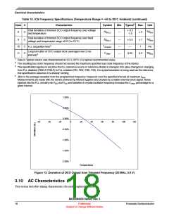
1.00%
0.50%
0.00%
-60
-40
-20
0
20
40
60
80
100
120
-0.50%
-1.00%
-1.50%
-2.00%
TBD
Temperature
Figure 13. Deviation of DCO Output from Trimmed Frequency (20 MHz, 3.0 V)
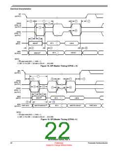
3.10 AC Characteristics
This section describes timing characteristics for each peripheral system.
MC9S08QE8 Series, Rev. 3
18
Preliminary
Freescale Semiconductor
Subject to Change Without Notice

 FREESCALE [ Freescale ]