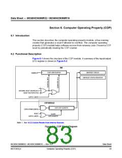
Data Sheet — MC68HC908MR32 • MC68HC908MR16
Section 5. Configuration Register (CONFIG)
5.1 Introduction
This section describes the configuration register (CONFIG). This register contains
bits that configure these options:
•
•
•
•
•
•
•
Resets caused by the low-voltage inhibit (LVI) module
Power to the LVI module
Computer operating properly (COP) module
Top-side pulse-width modulator (PWM) polarity
Bottom-side PWM polarity
Edge-aligned versus center-aligned PWMs
Six independent PWMs versus three complementary PWM pairs
5.2 Functional Description
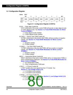
The configuration register (CONFIG) is used in the initialization of various options.
The configuration register can be written once after each reset. All of the
configuration register bits are cleared during reset. Since the various options affect
the operation of the microcontroller unit (MCU), it is recommended that this register
be written immediately after reset. The configuration register is located at $001F
and may be read at anytime.
NOTE:
On a FLASH device, the options are one-time writeable by the user after each
reset. The registers are not in the FLASH memory but are special registers
containing one-time writeable latches after each reset. Upon a reset, the
configuration register defaults to predetermined settings as shown in Figure 5-1.
If the LVI module and the LVI reset signal are enabled, a reset occurs when VDD
falls to a voltage, VLVRx, and remains at or below that level for at least nine
consecutive central processor unit (CPU) cycles. Once an LVI reset occurs, the
MCU remains in reset until VDD rises to a voltage, VLVRX
.
MC68HC908MR32 • MC68HC908MR16 — Rev. 6.0
MOTOROLA Configuration Register (CONFIG)
Data Sheet
79

 FREESCALE [ Freescale ]