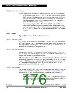
Serial Communications Interface Module (SCI)
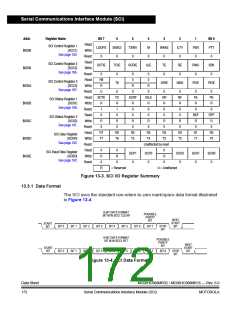
Addr.
Register Name
Bit 7
LOOPS
0
6
ENSCI
0
5
4
M
3
WAKE
0
2
ILTY
0
1
PEN
0
Bit 0
PTY
0
Read:
Write:
Reset:
Read:
Write:
Reset:
Read:
Write:
Reset:
SCI Control Register 1
(SCC1)
See page 183.
TXINV
0
$0038
0
SCI Control Register 2
(SCC2)
See page 185.
SCTIE
TCIE
0
SCRIE
ILIE
TE
RE
0
RWU
0
SBK
0
$0039
$003A
$003B
$003C
$003D
$003E
0
R8
R
0
0
0
0
0
SCI Control Register 3
(SCC3)
See page 187.
T8
ORIE
NEIE
FEIE
PEIE
R
R
U
U
TC
R
0
0
0
OR
R
0
NF
R
0
FE
R
0
PE
R
Read: SCTE
SCRF
R
IDLE
R
SCI Status Register 1
(SCS1)
See page 188.
Write:
Reset:
Read:
Write:
Reset:
Read:
Write:
Reset:
Read:
Write:
Reset:
R
1
1
0
0
0
0
0
0
0
0
0
0
0
0
BKF
R
RPF
R
SCI Status Register 2
(SCS2)
See page 191.
R
R
R
R
R
R
0
0
0
0
0
0
0
0
R7
T7
R6
T6
R5
T5
R4
T4
R3
T3
R2
T2
R1
T1
R0
T0
SCI Data Register
(SCDR)
See page 192.
Unaffected by reset
0
R
0
0
0
SCI Baud Rate Register
(SCBR)
See page 192.
SCP1
0
SCP0
R
SCR2
0
SCR1
0
SCR0
0
R
0
0
0
= Reserved
U = Unaffected
R
Figure 13-3. SCI I/O Register Summary
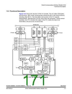
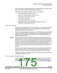
13.3.1 Data Format
The SCI uses the standard non-return-to-zero mark/space data format illustrated
in Figure 13-4.
8-BIT DATA FORMAT
POSSIBLE
PARITY
BIT M IN SCC1 CLEAR
NEXT
START
BIT
BIT
START
BIT
STOP
BIT
BIT 0
BIT 1
BIT 2
BIT 3
BIT 4
BIT 5
BIT 6
BIT 7
9-BIT DATA FORMAT
BIT M IN SCC1 SET
POSSIBLE
PARITY
BIT
NEXT
START
BIT
START
BIT
BIT 0
BIT 1
BIT 2
BIT 3
BIT 4
BIT 5
BIT 6
BIT 7
BIT 8
STOP
BIT
Figure 13-4. SCI Data Formats
Data Sheet
172
MC68HC908MR32 • MC68HC908MR16 — Rev. 6.0
Serial Communications Interface Module (SCI) MOTOROLA

 FREESCALE [ Freescale ]