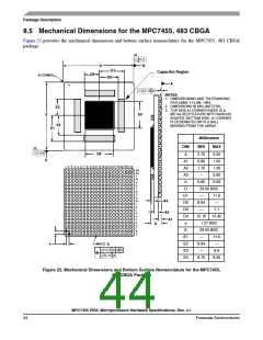
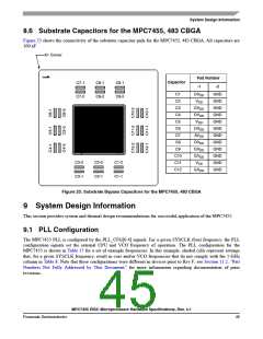
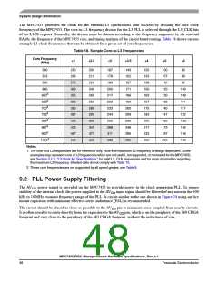
System Design Information
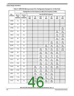
The MPC7455 generates the clock for the external L3 synchronous data SRAMs by dividing the core clock
frequency of the MPC7455. The core-to-L3 frequency divisor for the L3 PLL is selected through the L3_CLK bits
of the L3CR register. Generally, the divisor must be chosen according to the frequency supported by the external
RAMs, the frequency of the MPC7455 core, and timing analysis of the circuit board routing. Table 18 shows various
example L3 clock frequencies that can be obtained for a given set of core frequencies.
Table 18. Sample Core-to-L3 Frequencies
Core Frequency
÷2
÷2.5
÷3
÷3.5
÷4
÷5
÷6
(MHz)
500
533
550
600
250
266
275
300
325
333
350
367
400
433
467
500
200
213
220
240
260
266
280
293
320
347
373
400
167
178
183
200
217
222
233
244
266
289
311
333
143
152
157
171
186
190
200
209
230
248
266
285
125
133
138
150
163
167
175
183
200
217
233
250
100
107
110
120
130
133
140
147
160
173
187
200
83
89
92
100
108
111
117
122
133
145
156
166
2
650
2
666
2
700
2
733
2
800
2
867
2
933
2
1000
Notes:
1. The core and L3 frequencies are for reference only. Note that maximum L3 frequency is design dependent. Some
examples may represent core or L3 frequencies which are not useful, not supported, or not tested for the MPC7455;
see Section 5.2.3, “L3 Clock AC Specifications,” for valid L3_CLK frequencies and for more information regarding
the maximum L3 frequency. Shaded cells do not comply with Table 10.
2. These core frequencies are not supported by all speed grades; see Table 8.
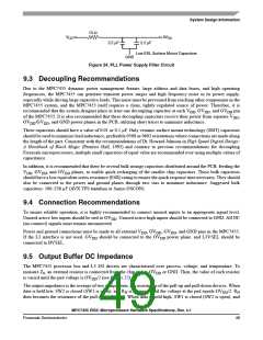
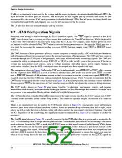
9.2 PLL Power Supply Filtering
The AV
power signal is provided on the MPC7455 to provide power to the clock generation PLL. To ensure
DD
stability of the internal clock, the power supplied to the AV input signal should be filtered of any noise in the 500
DD
kHz to 10 MHz resonant frequency range of the PLL. A circuit similar to the one shown in Figure 24 using surface
mount capacitors with minimum effective series inductance (ESL) is recommended.
The circuit should be placed as close as possible to the AV pin to minimize noise coupled from nearby circuits.
DD
It is often possible to route directly from the capacitors to the AV pin, which is on the periphery of the 360 CBGA
DD
footprint and very close to the periphery of the 483 CBGA footprint, without the inductance of vias.
MPC7455 RISC Microprocessor Hardware Specifications, Rev. 4.1
48
Freescale Semiconductor

 FREESCALE [ Freescale ]