I/O Registers
NOTE
Writing to the TE bit is not allowed when the enable SCI bit (ENSCI) is clear.
ENSCI is in SCI control register 1.
RE — Receiver Enable Bit
Setting this read/write bit enables the receiver. Clearing the RE bit disables the receiver but does not
affect receiver interrupt flag bits. Reset clears the RE bit.
1 = Receiver enabled
0 = Receiver disabled
NOTE
Writing to the RE bit is not allowed when the enable SCI bit (ENSCI) is
clear. ENSCI is in SCI control register 1.
RWU — Receiver Wakeup Bit
This read/write bit puts the receiver in a standby state during which receiver interrupts are disabled.
The WAKE bit in IRSCC1 determines whether an idle input or an address mark brings the receiver out
of the standby state and clears the RWU bit. Reset clears the RWU bit.
1 = Standby state
0 = Normal operation
SBK — Send Break Bit
Setting and then clearing this read/write bit transmits a break character followed by a logic 1. The logic
1 after the break character guarantees recognition of a valid start bit. If SBK remains set, the
transmitter continuously transmits break characters with no logic 1s between them. Reset clears the
SBK bit.
1 = Transmit break characters
0 = No break characters being transmitted
NOTE
Do not toggle the SBK bit immediately after setting the SCTE bit. Toggling
SBK before the preamble begins causes the SCI to send a break character
instead of a preamble.
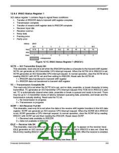
12.9.3 IRSCI Control Register 3
IRSCI control register 3:
•
•
Stores the ninth SCI data bit received and the ninth SCI data bit to be transmitted
Enables the following interrupts:
–
–
–
–
Receiver overrun interrupts
Noise error interrupts
Framing error interrupts
Parity error interrupts
Address:
$0042
Bit 7
R8
6
T8
U
5
DMARE
0
4
DMATE
0
3
2
NEIE
0
1
FEIE
0
Bit 0
PEIE
0
Read:
Write:
Reset:
ORIE
U
0
= Unimplemented
U = Unaffected
Figure 12-14. IRSCI Control Register 3 (IRSCC3)
MC68HC908AP Family Data Sheet, Rev. 4
Freescale Semiconductor
201

 FREESCALE [ Freescale ]