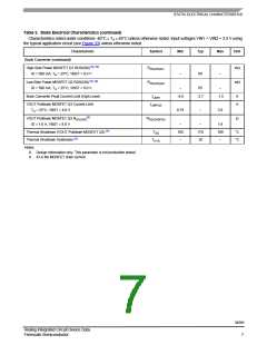
STATIC ELECTRICAL CHARACTERISTICS
Table 3. Static Electrical Characteristics (continued)
Characteristics noted under conditions -40°C ≤ TA ≤ 85°C unless otherwise noted. Input voltages VIN1 = VIN2 = 3.3 V using
the typical application circuit (see Figure 33) unless otherwise noted.
Characteristic
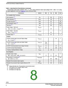
Error Amplifier (Buck Converter)
Symbol
Min
Typ
Max
Unit
Input Impedance (10)
Output Impedance (10)
DC Open Loop Gain (10)
Gain Bandwidth Product (10)
Slew Rate (10)
R
–
–
–
–
–
500
150
80
–
–
–
–
–
kΩ
Ω
IN
R
OUT
A
dB
VOL
GBW
35
MHz
V/µs
V
200
v
SR
Output Voltage – High Level
V
V
EA_OH
VIN1 > 3.3 V, IOEA = -1.0 mA (10), (11)
–
2.0
–
Output Voltage – Low Level
IOEA = -1.0 mA (10), (11)
V
V
EA_OL
–
–
0.4
0.5
–
–
Oscillator Ramp (10)
V
V
SCRamp
Oscillator
CLKSYN Terminal (open) Low Level Output Voltage
IOL = +1.0 mA (12)
–
–
0.4
V
V
OSC_OL
CLKSYN Terminal (open) High Level Output Voltage
IOH = -1.0 mA (13)
V
VDDI
OSC_OH
- 0.4 V
–
–
CLKSYN Terminal (grounded) Input Voltage Threshold
CLKSYN Terminal Pullup Resistance
Frequency Adjusting Reference Voltage
Boost Regulator
V
1.2
60
–
–
–
2.0
240
–
V
kΩ
V
OSC_IH
RPU
V
1.26
FREQ
Regulator Output Voltage
V
V
BST
7.3
–
7.7
8.3
IBST = 20 mA, VIN1 = VIN2 = 2.8 V to 6.0 V
Power MOSFET Q5 RDS(ON)(10)
R
mΩ
DS(ON)Q5
CBST
IBD = 500 mA, T = 25°C
A
650
1000
Regulator Recommended Output Capacitor
–
–
10
–
–
µF
Regulator Recommended Output Capacitor Maximum ESR
ESRCBST
100
mΩ
Notes
10. Design information only. This parameter is not production tested.
11. IOEA Refers to Error Amplifier Output Current.
12. IOL Refers to I/O Low Level
13. IOH Refers to I/O High Level
34701
Analog Integrated Circuit Device Data
Freescale Semiconductor
8

 FREESCALE [ Freescale ]