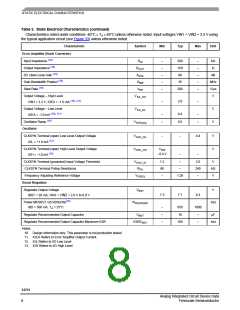
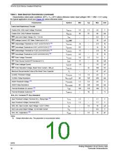
DYNAMIC ELECTRICAL CHARACTERISTICS
Table 4. DYNAMIC ELECTRICAL CHARACTERISTICS (continued)
Characteristics noted under conditions -40°C ≤ TA ≤ 85°C unless otherwise noted. Input voltages VIN1 = VIN2 = 3.3 V using
the typical application circuit (see Figures 33) unless otherwise noted.
Characteristic
Symbol
Min
Typ
Max
Unit
Boost Regulator
Boost Regulator MOSFET Maximum ON Time (20)
Boost Regulator Control Loop Propagation Delay (20)
t
–
–
24
50
–
–
µs
ns
ns
ON
t
BST_PD
Boost Switching Node VBD Rise Time (20)
IBST = 20 mA
t
B_RISE
–
–
5.0
3.0
Boost Switching Node VBD Fall Time (20)
IBST = 20 mA
t
ns
B_FALL
–
Linear Regulator (LDO)
Fault Condition Time-Out
Retry Timer Cycle
t
7.0
70
10
15
ms
ms
FAULT
t
100
150
Ret
Reset Monitor (RST)
Monitoring LFB Terminal Delay
Monitoring INV Terminal Delay
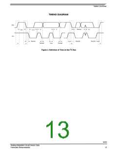
SCA, SCL Terminal, I2C Bus (Standard)
t
12
12
–
–
28
28
µs
µs
D_RST_LFB
t
D_RST_INV
SCL Clock Frequency (20)
SCL
f
–
–
–
100
–
kHz
µs
Bus Free Time Between a STOP and a START Condition (20)
BUF
t
4.7
Hold Time (Repeated) START Condition (After this period, the first clock
pulse is generated.) (20)
t
µs
HD-STA
4.0
4.7
4.0
–
–
–
–
–
–
Low Period of the SCL Clock (20)
High Period of the SCL Clock (20)
LOW
t
µs
µs
ns
t
HIGH
SDA Fall Time from VIH_MAX to VIL_MIN, Bus Capacitance 10 pF to 400
pF, 3.0 mA Sink Current (20), (22)
t
F
–
–
–
–
–
–
–
250
–
Setup Time for a Repeated START Condition (20)
SU-STA
t
4.7
0.0
250
4.0
–
µs
µs
ns
µs
pF
(21)
Data Hold Time for I2C Bus Devices (20)
Data Setup Time (20)
,
HD-DAT
T
t
t
–
–
SU-DA
Setup Time for STOP Condition (20)
SU-STO
CB
t
–
Capacitive Load for Each Bus Line (20)
400
Notes
20. Design information only. This parameter is not production tested.
21. The device provides an internal hold time of at least 300 ns for the SDA signal (refer to the VIH_MIN of the SCL signal) to bridge the
undefined region of the falling edge of SCL.
22. VIH is High Level Voltage on I2C bus lines and VIL is Low Level Voltage on I2C bus lines
34701
Analog Integrated Circuit Device Data
Freescale Semiconductor
12

 FREESCALE [ Freescale ]