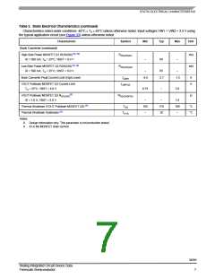
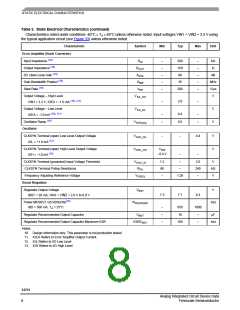
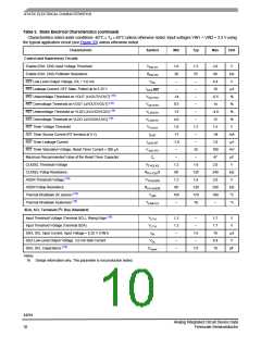
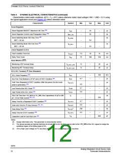
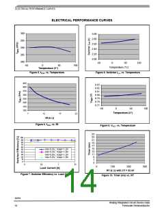
DYNAMIC ELECTRICAL CHARACTERISTICS
DYNAMIC ELECTRICAL CHARACTERISTICS
Table 4. DYNAMIC ELECTRICAL CHARACTERISTICS
Characteristics noted under conditions -40°C ≤ TA ≤ 85°C unless otherwise noted. Input voltages VIN1 = VIN2 = 3.3 V using
the typical application circuit (see Figures 33) unless otherwise noted.
Characteristic
Symbol
Min
Typ
Max
Unit
Buck Converter
Duty Cycle Range (Normal Operation) (17)
t
0
–
–
95
–
%
D
Switching Node SW Rise Time (17)
VIN = 5.0 V, ILOAD = 1.0 A
t
ns
RISE
7.0
Switching Node SW Fall Time (17)
VIN = 5.0 V, ILOAD = 1.0 A
t
ns
FALL
–
–
17
35
–
–
Maximum Deadtime (17)
t
ns
ns
D
Buck Control Loop Propagation Delay (17)
t
PD
VINV < 0.8 V to VSW > 90% of High Level or VINV > 0.8 V to VSW < 10%
of Low Level
–
50
350
10
–
Soft Start Duration (Power Sequencing Disabled, EN1 = 1, EN2 = 1) (17)
t
200
7.0
70
800
15
µs
ms
ms
SS
Fault Condition Time-Out (17)
Retry Timer Cycle (17)
Oscillator
t
FAULT
t
100
150
RET
Oscillator Center Frequency(19)
f
270
300
330
kHz
OSC
RF = 11.3 kΩ
Oscillator Frequency Range
f
200
7.0
–
–
400
22
kHz
kΩ
OSC
Oscillator Frequency Adjusting Resistor Range
R
FREQ
Oscillator Frequency Adjustment (18), (19)
f
kHz
OSC
OSC
OSC
RF = 7.0 kΩ
400
–
–
Oscillator Frequency Adjustment (18), (19)
f
f
kHz
RF = 22 kΩ
–
–
–
200
–
Oscillator Default Frequency (Switching Frequency), FREQ Terminal Open
300
kHz
%
Oscillator Output Signal Duty Cycle (Square Wave, 180° Out-of-Phase with
the Internal Suitable Oscillator)
D
OSC
40
50
–
60
–
Synchronization Pulse Minimum Duration (17)
t
1.0
µs
SYNC
Notes
17. Design information only. This parameter is not production tested.
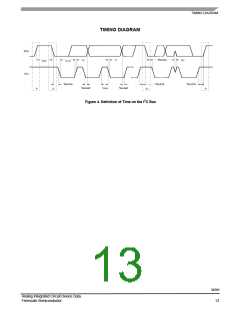
18. see Figure 4 for more details
19. RF is RFREQ
34701
Analog Integrated Circuit Device Data
Freescale Semiconductor
11

 FREESCALE [ Freescale ]