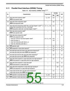
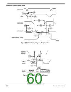
Parallel Host Interface (HDI08) Timing
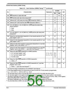
Table 3-15 Host Interface (HDI08) Timing1, 2, 3 (continued)
150 MHz
No.
Characteristics
Expression
Unit
Min
Max
19.1
—
332 HCS assertion to output data valid
—
—
—
—
—
ns
ns
ns
ns
ns
333 HCS hold time after data strobe deassertion9
0.0
4.7
3.3
334 Address (AD7–AD0) setup time before HAS deassertion (HMUX=1)
335 Address (AD7–AD0) hold time after HAS deassertion (HMUX=1)
—
—
336 A10–A8 (HMUX=1), A2–A0 (HMUX=0), HR/W setup time before data
strobe assertion9
• Read
• Write
—
0
—
—
4.7
337 A10–A8 (HMUX=1), A2–A0 (HMUX=0), HR/W hold time after data strobe
deassertion9
—
TC
3.3
6.7
13.4
—
—
ns
ns
ns
ns
ns
ns
338 Delay from read data strobe deassertion to host request assertion for “Last
Data Register” read4, 5, 10
—
339 Delay from write data strobe deassertion to host request assertion for “Last
Data Register” write5, 8, 10
2 × TC
—
—
340 Delay from data strobe assertion to host request deassertion for “Last Data
Register” read or write (HROD = 0)5, 9, 10
19.1
300.0
341 Delay from data strobe assertion to host request deassertion for “Last Data
Register” read or write (HROD = 1, open drain Host Request)5, 9, 10, 11
—
—
342 Delay from DMA HACK deassertion to HOREQ assertion
• For “Last Data Register” read5
2 × TC + 19.1
32.5
—
—
—
• For “Last Data Register” write5
1.5 × TC + 19.1 29.2
• For other cases
0.0
343 Delay from DMA HACK assertion to HOREQ deassertion
• HROD = 05
—
—
—
—
20.2
ns
ns
344 Delay from DMA HACK assertion to HOREQ deassertion for “Last Data
Register” read or write
300.0
• HROD = 1, open drain Host Request5, 11
1
2
3
4
5
6
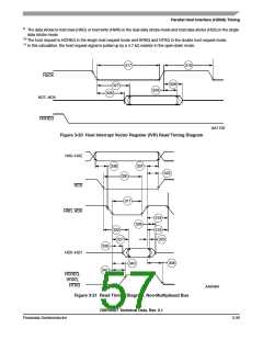
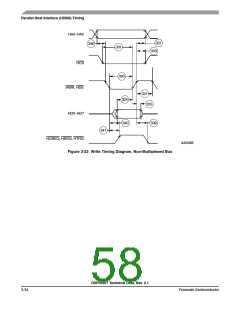
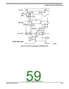
See Host Port Usage Considerations in the DSP56367 User’s Manual.
In the timing diagrams below, the controls pins are drawn as active low. The pin polarity is programmable.
VCC = 1.8 V 5%; TJ = –40°C to +95°C, CL = 50 pF
The read data strobe is HRD in the dual data strobe mode and HDS in the single data strobe mode.
The “last data register” is the register at address $7, which is the last location to be read or written in data transfers.
This timing is applicable only if a read from the “last data register” is followed by a read from the RXL, RXM, or RXH registers
without first polling RXDF or HREQ bits, or waiting for the assertion of the HOREQ signal.
7
8
This timing is applicable only if two consecutive reads from one of these registers are executed.
The write data strobe is HWR in the dual data strobe mode and HDS in the single data strobe mode.
DSP56367 Technical Data, Rev. 2.1
3-32
Freescale Semiconductor

 FREESCALE [ Freescale ]