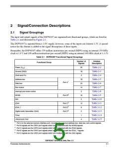
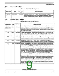
2 Signal/Connection Descriptions
2.1
Signal Groupings
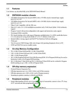
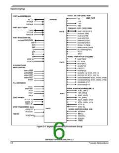
The input and output signals of the DSP56367 are organized into functional groups, which are listed in
Table 2-1 and illustrated in Figure 2-1.
The DSP56367 is operated from a 1.8V supply; however, some of the inputs can tolerate 3.3V. A special
notice for this feature is added to the signal descriptions of those inputs.
Remember, the DSP56367 offers 150 million instructions per second (MIPS) using an internal 150 MHz
clock at 1.8 V and 100 million instructions per second (MIPS) using an internal 100 MHz clock at 1.3.3V.
Table 2-1 DSP56367 Functional Signal Groupings
Number of
Signals
Detailed
Description
Functional Group
Power (VCC
)
20
18
3
Table 2-2
Table 2-3
Table 2-4
Table 2-5
Table 2-6
Table 2-7
Table 2-8
Table 2-9
Table 2-10
Table 2-11
Table 2-12
Table 2-13
Table 2-14
Table 2-15
Ground (GND)
Clock and PLL
Address bus
Data bus
18
24
10
5
Port A1
Bus control
Interrupt and mode control
HDI08
Port B2
16
5
SHI
ESAI
Port C3
Port E4
Port D5
12
6
ESAI_1
Digital audio transmitter (DAX)
Timer
2
1
JTAG/OnCE Port
4
1
2
3
4
5
Port A is the external memory interface port, including the external address bus, data bus, and control signals.
Port B signals are the GPIO port signals which are multiplexed with the HDI08 signals.
Port C signals are the GPIO port signals which are multiplexed with the ESAI signals.
Port E signals are the GPIO port signals which are multiplexed with the ESAI_1 signals.
Port D signals are the GPIO port signals which are multiplexed with the DAX signals.
DSP56367 Technical Data, Rev. 2.1
Freescale Semiconductor
2-1

 FREESCALE [ Freescale ]