Overview
1.1
Features
Core features are described fully in the DSP56300 Family Manual.
1.2
DSP56300 modular chassis
•
150 Million Instructions Per Second (MIPS) with a 150 MHz clock at internal logic supply
(QVCCL) of 1.8V.
•
100 Million Instructions Per Second (MIPS) with a 100 MHz clock at internal logic supply
(QVCCL) of 1.5V.
•
•
Object Code Compatible with the 56K core.
Data ALU with a 24 × 24 bit multiplier-accumulator and a 56-bit barrel shifter. 16-bit arithmetic
support.
•
•
•
Program Control with position independent code support and instruction cache support.
Six-channel DMA controller.
PLL based clocking with a wide range of frequency multiplications (1 to 4096), predivider factors
i
(1 to 16) and power saving clock divider (2 : i=0 to 7). Reduces clock noise.
•
•
•
•
Internal address tracing support and OnCE™ for Hardware/Software debugging.
JTAG port.
Very low-power CMOS design, fully static design with operating frequencies down to DC.
STOP and WAIT low-power standby modes.
1.3
On-chip Memory Configuration
•
•
•
•
7K × 24 Bit Y-Data RAM and 8K × 24 Bit Y-Data ROM.
13K × 24 Bit X-Data RAM and 32K × 24 Bit X-Data ROM.
40K × 24 Bit Program ROM.
3K × 24 Bit Program RAM and 192x24 Bit Bootstrap ROM. 1K of Program RAM may be used as
Instruction Cache or for Program ROM patching.
•
2K × 24 Bit from Y Data RAM and 5K × 24 Bit from X Data RAM can be switched to Program
RAM resulting in up to 10K × 24 Bit of Program RAM.
1.4
Off-chip memory expansion
•
•
•
•
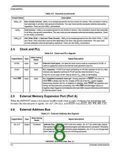
External Memory Expansion Port.
Off-chip expansion up to two 16M x 24-bit word of Data memory.
Off-chip expansion up to 16M x 24-bit word of Program memory.
Simultaneous glueless interface to SRAM and DRAM.
1.5
Peripheral modules
Serial Audio Interface (ESAI): up to 4 receivers and up to 6 transmitters, master or slave. I S, Sony,
2
•
AC97, network and other programmable protocols.
DSP56367 Technical Data, Rev. 2.1
Freescale Semiconductor
1-3

 FREESCALE [ Freescale ]