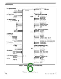
Clock and PLL
Table 2-3 Grounds (continued)
Description
Ground Name
GNDC (2)
Bus Control Ground—GNDC is an isolated ground for the bus control I/O drivers. This connection must be
tied externally to all other chip ground connections. The user must provide adequate external decoupling
capacitors. There are two GNDC connections.
GNDH
Host Ground—GNDh is an isolated ground for the HD08 I/O drivers. This connection must be tied externally
to all other chip ground connections. The user must provide adequate external decoupling capacitors. There
is one GNDH connection.
GNDS (2)
SHI, ESAI, ESAI_1, DAX and Timer Ground—GNDS is an isolated ground for the SHI, ESAI, ESAI_1, DAX
and Timer. This connection must be tied externally to all other chip ground connections. The user must
provide adequate external decoupling capacitors. There are two GNDS connections.
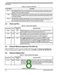
2.4
Clock and PLL
Table 2-4 Clock and PLL Signals
Signal Description
State During
Signal Name Type
Reset
EXTAL
Input
Input
Input
External Clock Input—An external clock source must be connected to EXTAL in
order to supply the clock to the internal clock generator and PLL.
PCAP
Input
Input
PLL Capacitor—PCAP is an input connecting an off-chip capacitor to the PLL filter.
Connect one capacitor terminal to PCAP and the other terminal to VCCP
.
If the PLL is not used, PCAP may be tied to VCC, GND, or left floating.
PINIT/NMI
Input
PLL Initial/Nonmaskable Interrupt—During assertion of RESET, the value of
PINIT/NMI is written into the PLL Enable (PEN) bit of the PLL control register,
determining whether the PLL is enabled or disabled. After RESET de assertion and
during normal instruction processing, the PINIT/NMI Schmitt-trigger input is a
negative-edge-triggered nonmaskable interrupt (NMI) request internally synchronized
to internal system clock.
2.5
External Memory Expansion Port (Port A)
When the DSP56367 enters a low-power standby mode (stop or wait), it releases bus mastership and
tri-states the relevant port A signals: A0–A17, D0–D23, AA0/RAS0–AA2/RAS2, RD, WR, BB, CAS.
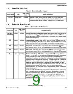
2.6
External Address Bus
Table 2-5 External Address Bus Signals
State During
Reset
Signal Name Type
A0–A17 Output
Signal Description
Tri-Stated
Address Bus—When the DSP is the bus master, A0–A17 are active-high outputs
that specify the address for external program and data memory accesses. Otherwise,
the signals are tri-stated. To minimize power dissipation, A0–A17 do not change state
when external memory spaces are not being accessed.
DSP56367 Technical Data, Rev. 2.1
2-4
Freescale Semiconductor

 FREESCALE [ Freescale ]