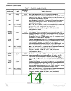
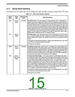
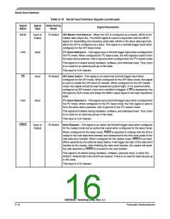
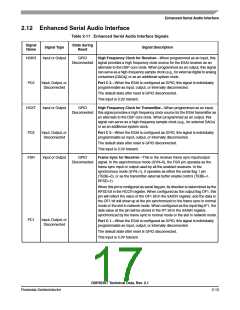
Enhanced Serial Audio Interface
Table 2-11 Enhanced Serial Audio Interface Signals (continued)
Signal
Name
State during
Reset
Signal Type
Signal Description
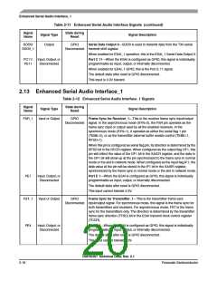
FST
PC4
Input or Output
GPIO
Frame Sync for Transmitter—This is the transmitter frame sync input/output
Disconnected signal. For synchronous mode, this signal is the frame sync for both
transmitters and receivers. For asynchronous mode, FST is the frame sync for
the transmitters only. The direction is determined by the transmitter frame
sync direction (TFSD) bit in the ESAI transmit clock control register (TCCR).
Input, Output, or
Disconnected
Port C 4—When the ESAI is configured as GPIO, this signal is individually
programmable as input, output, or internally disconnected.
The default state after reset is GPIO disconnected.
This input is 3.3V tolerant.
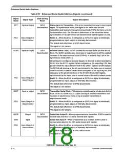
SCKR
Input or Output
GPIO
Receiver Serial Clock—SCKR provides the receiver serial bit clock for the
Disconnected ESAI. The SCKR operates as a clock input or output used by all the enabled
receivers in the asynchronous mode (SYN=0), or as serial flag 0 pin in the
synchronous mode (SYN=1).
When this pin is configured as serial flag pin, its direction is determined by the
RCKD bit in the RCCR register. When configured as the output flag OF0, this
pin will reflect the value of the OF0 bit in the SAICR register, and the data in
the OF0 bit will show up at the pin synchronized to the frame sync in normal
mode or the slot in network mode. When configured as the input flag IF0, the
data value at the pin will be stored in the IF0 bit in the SAISR register,
synchronized by the frame sync in normal mode or the slot in network mode.
PC0
Input, Output, or
Disconnected
Port C 0—When the ESAI is configured as GPIO, this signal is individually
programmable as input, output, or internally disconnected.
The default state after reset is GPIO disconnected.
This input is 3.3V tolerant.
SCKT
PC3
Input or output
GPIO
Transmitter Serial Clock—This signal provides the serial bit rate clock for the
Disconnected ESAI. SCKT is a clock input or output used by all enabled transmitters and
receivers in synchronous mode, or by all enabled transmitters in
asynchronous mode.
Input, Output, or
Disconnected
Port C 3—When the ESAI is configured as GPIO, this signal is individually
programmable as input, output, or internally disconnected.
The default state after reset is GPIO disconnected.
This input is 3.3V tolerant.
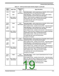
SDO5
SDI0
PC6
Output
Input
GPIO
Serial Data Output 5—When programmed as a transmitter, SDO5 is used to
Disconnected transmit data from the TX5 serial transmit shift register.
Serial Data Input 0—When programmed as a receiver, SDI0 is used to
receive serial data into the RX0 serial receive shift register.
Input, Output, or
Disconnected
Port C 6—When the ESAI is configured as GPIO, this signal is individually
programmable as input, output, or internally disconnected.
The default state after reset is GPIO disconnected.
This input is 3.3V tolerant.
DSP56367 Technical Data, Rev. 2.1
2-14
Freescale Semiconductor

 FREESCALE [ Freescale ]