Serial Host Interface
2.11 Serial Host Interface
2
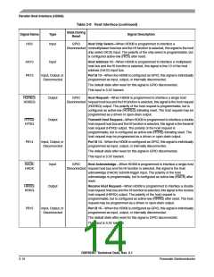
The SHI has five I/O signals that can be configured to allow the SHI to operate in either SPI or I C mode.
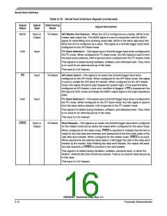
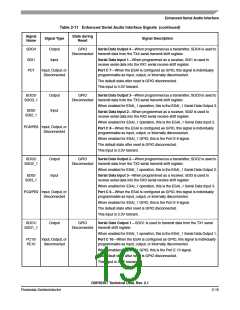
Table 2-10 Serial Host Interface Signals
Signal
Name
Signal
Type
State During
Reset
Signal Description
SCK
Input or
Output
Tri-Stated
SPI Serial Clock—The SCK signal is an output when the SPI is configured as a
master and a Schmitt-trigger input when the SPI is configured as a slave. When the
SPI is configured as a master, the SCK signal is derived from the internal SHI clock
generator. When the SPI is configured as a slave, the SCK signal is an input, and
the clock signal from the external master synchronizes the data transfer. The SCK
signal is ignored by the SPI if it is defined as a slave and the slave select (SS) signal
is not asserted. In both the master and slave SPI devices, data is shifted on one
edge of the SCK signal and is sampled on the opposite edge where data is stable.
Edge polarity is determined by the SPI transfer protocol.
SCL
Input or
Output
I2C Serial Clock—SCL carries the clock for I2C bus transactions in the I2C mode.
SCL is a Schmitt-trigger input when configured as a slave and an open-drain output
when configured as a master. SCL should be connected to VCC through a pull-up
resistor.
This signal is tri-stated during hardware, software, and individual reset. Thus, there
is no need for an external pull-up in this state.
This input is 3.3V tolerant.
MISO
SDA
Input or
Output
Tri-Stated
SPI Master-In-Slave-Out—When the SPI is configured as a master, MISO is the
master data input line. The MISO signal is used in conjunction with the MOSI signal
for transmitting and receiving serial data. This signal is a Schmitt-trigger input when
configured for the SPI Master mode, an output when configured for the SPI Slave
mode, and tri-stated if configured for the SPI Slave mode when SS is deasserted.
An external pull-up resistor is not required for SPI operation.
Input or
Open-Drain
Output
I2C Data and Acknowledge—In I2C mode, SDA is a Schmitt-trigger input when
receiving and an open-drain output when transmitting. SDA should be connected to
V
CC through a pull-up resistor. SDA carries the data for I2C transactions. The data
in SDA must be stable during the high period of SCL. The data in SDA is only
allowed to change when SCL is low. When the bus is free, SDA is high. The SDA
line is only allowed to change during the time SCL is high in the case of start and
stop events. A high-to-low transition of the SDA line while SCL is high is a unique
situation, and is defined as the start event. A low-to-high transition of SDA while
SCL is high is a unique situation defined as the stop event.
This signal is tri-stated during hardware, software, and individual reset. Thus, there
is no need for an external pull-up in this state.
This input is 3.3V tolerant.
DSP56367 Technical Data, Rev. 2.1
Freescale Semiconductor
2-11

 FREESCALE [ Freescale ]