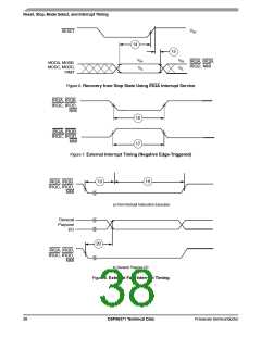
Reset, Stop, Mode Select, and Interrupt Timing
Table 19. Reset, Stop, Mode Select, and Interrupt Timing (Continued)
No.
Characteristics
Interrupt Requests Rate
Expression
Min
Max
Unit
21
12 x TC
• ESAI, ESAI_1, SHI, DAX, Timer
—
—
—
—
—
—
—
—
ns
ns
ns
ns
• DMA
8 x TC
8 x TC
12 c TC
• IRQ, NMI (edge trigger)
• IRQ (level trigger)
22
DMA Requests Rate
6 x TC
—
ns
• Data read from ESAI, ESAI_1, SHI, DAX
—
—
—
—
• Data write to ESAI, ESAI_1, SHI, DAX
• Timer
7 x TC
2 x TC
3 x TC
—
—
—
ns
ns
ns
• IRQ, NMI (edge trigger)
Notes:
1. When using fast interrupts and IRQA, IRQB, IRQC, and IRQD are defined as level-sensitive, timings 19 through 21 apply
to prevent multiple interrupt service. To avoid these timing restrictions, the deasserted Edge-triggered mode is
recommended when using fast interrupts. Long interrupts are recommended when using Level-sensitive mode.
2. For PLL disable, using external clock (PCTL Bit 13 = 0), no stabilization delay is required and recovery time will be
defined by the OMR Bit 6 settings.
For PLL enable, (if bit 12 of the PCTL register is 0), the PLL is shutdown during Stop. Recovering from Stop requires the
PLL to get locked. The PLL lock procedure duration, PLL Lock Cycles (PLC), may be in the range of 0.5 ms.
3. Periodically sampled and not 100% tested
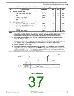
4. RESET duration is measured during the time in which RESET is asserted, VDD is valid, and the EXTAL input is active
and valid. When the VDD is valid, but the other “required RESET duration” conditions (as specified above) have not been
yet met, the device circuitry will be in an uninitialized state that can result in significant power consumption and heat-up.
Designs should minimize this state to the shortest possible duration.
VIH
RESET
11
13
10
All Pins
Reset Value
Figure 5. Reset Timing
Freescale Semiconductor
DSP56371 Technical Data
37

 FREESCALE [ Freescale ]