Signal/Connection Descriptions
Table 6. Interrupt and Mode Control (Continued)
State
Signal Name
Type
During
Reset
Signal Description
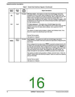
RESET
Input
Input
Reset—RESET is an active-low, Schmitt-trigger input. When asserted, the
chip is placed in the Reset state and the internal phase generator is reset. The
Schmitt-trigger input allows a slowly rising input (such as a capacitor charging)
to reset the chip reliably. When the RESET signal is deasserted, the initial chip
operating mode is latched from the MODA, MODB, MODC and MODD inputs.
The RESET signal must be asserted during power up. A stable EXTAL signal
must be supplied while RESET is being asserted.
Internal Pull up resistor.
This input is 5 V tolerant.
3.7
Serial Host Interface
The SHI has five I/O signals that can be configured to allow the SHI to operate in either SPI or I2C mode.
Table 7. Serial Host Interface Signals
State
during
Reset
Signal
Name
Signal
Type
Signal Description
SCK
Input or
output
Tri-stated SPI Serial Clock—The SCK signal is an output when the SPI is configured as a
master and a Schmitt-trigger input when the SPI is configured as a slave. When
the SPI is configured as a master, the SCK signal is derived from the internal
SHI clock generator. When the SPI is configured as a slave, the SCK signal is
an input, and the clock signal from the external master synchronizes the data
transfer. The SCK signal is ignored by the SPI if it is defined as a slave and the
slave select (SS) signal is not asserted. In both the master and slave SPI
devices, data is shifted on one edge of the SCK signal and is sampled on the
opposite edge where data is stable. Edge polarity is determined by the SPI
transfer protocol.
SCL
Input or
output
I2C Serial Clock—SCL carries the clock for I2C bus transactions in the I2C
mode. SCL is a Schmitt-trigger input when configured as a slave and an open-
drain output when configured as a master. SCL should be connected to VDD
through a pull-up resistor.
This signal is tri-stated during hardware, software and individual reset. Thus,
there is no need for an external pull-up in this state.
Internal Pull up resistor.
This input is 5 V tolerant.
14
DSP56371 Technical Data
Freescale Semiconductor

 FREESCALE [ Freescale ]