Signal/Connection Descriptions
3.3
Ground
Table 3. Grounds
Description
Ground Name
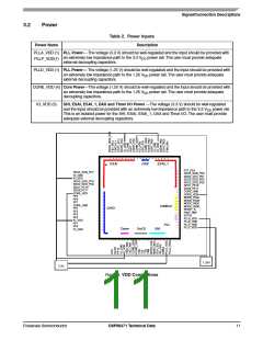
PLLA_GND(1) PLL Ground—The PLL ground should be provided with an extremely low-impedance path to
ground. The user must provide adequate external decoupling capacitors.
PLLP_GND(1)
PLLD_GND(1) PLL Ground—The PLL ground should be provided with an extremely low-impedance path to
ground. The user must provide adequate external decoupling capacitors.
CORE_GND (4) Core Ground—The Core ground should be provided with an extremely low-impedance path to
ground. This connection must be tied externally to all other chip ground connections. The user
must provide adequate external decoupling capacitors.
IO_GND (5)
SHI, ESAI, ESAI_1, DAX and Timer I/O Ground—IO_GND is an isolated ground for the SHI,
ESAI, ESAI_1, DAX and Timer I/O. This connection must be tied externally to all other chip ground
connections. The user must provide adequate external decoupling capacitors.
3.4
SCAN
Table 4. SCAN signals
State
Signal
Name
Type
during
Reset
Signal Description
SCAN—Manufacturing test pin. This pin should be pulled low.
Internal Pull down resistor.
SCAN
Input
Input
3.5
Clock and PLL
Table 5. Clock and PLL Signals
Signal Description
State
during
Reset
Signal
Name
Type
EXTAL
Input
Input
External Clock Input—An external clock source must be connected to EXTAL
in order to supply the clock to the internal clock generator and PLL.
This input cannot tolerate 5 V.
PINIT/NMI
Input
Input
PLL Initial/Nonmaskable Interrupt—During assertion of RESET, the value of
PINIT/NMI is written into the PLL Enable (PEN) bit of the PLL control register,
determining whether the PLL is enabled or disabled. After RESET de assertion
and during normal instruction processing, the PINIT/NMI Schmitt-trigger input is
a negative-edge-triggered nonmaskable interrupt (NMI) request internally
synchronized to internal system clock.
Internal Pull up resistor.
This input is 5 V tolerant.
3.6
Interrupt and Mode Control
The interrupt and mode control signals select the chip’s operating mode as it comes out of hardware reset. After RESET is
deasserted, these inputs are hardware interrupt request lines.
12
DSP56371 Technical Data
Freescale Semiconductor

 FREESCALE [ Freescale ]