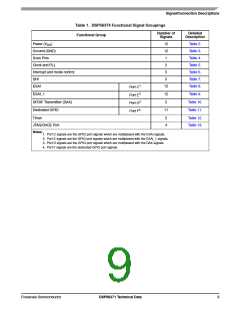
Signal/Connection Descriptions
3.2
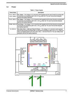
Power
Table 2. Power Inputs
Description
Power Name
PLLA_VDD (1) PLL Power— The voltage (3.3 V) should be well-regulated and the input should be provided with
an extremely low impedance path to the 3.3 VDD power rail. The user must provide adequate
external decoupling capacitors.
PLLP_VDD(1)
PLLD_VDD (1) PLL Power— The voltage (1.25 V) should be well-regulated and the input should be provided with
an extremely low impedance path to the 1.25 VDD power rail. The user must provide adequate
external decoupling capacitors.
CORE_VDD (4) Core Power—The voltage (1.25 V) should be well-regulated and the input should be provided with
an extremely low impedance path to the 1.25 VDD power rail. The user must provide adequate
decoupling capacitors.
IO_VDD (5)
SHI, ESAI, ESAI_1, DAX and Timer I/O Power —The voltage (3.3 V) should be well-regulated
and the input should be provided with an extremely low impedance path to the 3.3 VDD power rail.
This is an isolated power for the SHI, ESAI, ESAI_1, DAX and Timer I/O. The user must provide
adequate external decoupling capacitors.
ESAI
DAX
ESAI_1
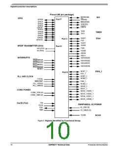
60
59
58
57
56
55
54
53
52
51
50
49
48
47
46
45
44
43
42
41
FST_PE4
SDO5_SDI0_PC7
IO_GND
IO_VDD
SDO3_SDI2_PC8
SDO2_SDI3_PC9
SDO1_PC10
SDO0_PC11
CORE_VDD
PF8
PF6
PF7
CORE_GND
PF2
PF3
1
2
SDO5_SDI0_PE6
SDO4_SDI1_PE7
SDO3_SDI2_PE8
SDO2_SDI3_PE9
SDO1_PE10
SDO0_PE11
CORE_GND
CORE_VDD
MODB_IRQA
MODB_IRQB
MODC_IRQC
MODD_IRQD
RESET_B
PINIT_NMI
EXTAL
PLLD_VDD
PLLD_GND
PLLP_GND
PLLP_VDD
3
4
5
6
7
8
9
10
11
12
13
14
15
16
17
18
19
20
Int/Mod
PLL
GPIO
PF4
PF5
IO_VDD
PF1
PF0
Timer
OnCE
SHI
IO_GND
1.25V
3.3V
Figure 3. VDD Connections
Freescale Semiconductor
DSP56371 Technical Data
11

 FREESCALE [ Freescale ]