Freescale Semiconductor, Inc.
Table 9-1. Boundary Scan Control Bits
Name
tout2.ctl
irq7.ctl
irq6.ctl
irq5.ctl
cs3.ctl
irq3.ctl
cs2.ctl
cs1.ctl
Bit Number
Name
cs0.ctl
ab.ctl
Bit Number
Name
ab28.ctl
ab29.ctl
ab30.ctl
ab31.ctl
modck.ctl
ifetch.ctl
tout1.ctl
Bit Number
29
52
54
56
58
60
62
64
66
83
84
85
87
89
91
93
95
97
berr.ctl
db.ctl
99
101
122
125
130
ab24.ctl
ab25.ctl
ab26.ctl
ab27.ctl
Boundary scan bit definitions are shown in Table 9-2. The first column in Table 9-2 defines
the bit's ordinal position in the boundary scan register. The shift register bit nearest TDO
(i.e., first to be shifted out) is defined as bit 0; the last bit to be shifted out is 131.
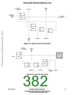
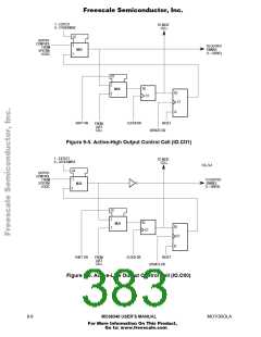
The second column references one of the five MC68340 cell types depicted in Figures
9-3–9-7, which describe the cell structure for each type.
The third column lists the pin name for all pin-related bits or defines the name of
bidirectional control register bits. The active level of the control bits (i.e., output driver on)
is defined by the last digit of the cell type listed for each control bit. For example, the
active-high level for irq7.ctl (bit 52) is logic zero since the cell type is IO.Ctl0. The active
level for ab.ctl (bit 83) is logic one, since the cell type is IO.Ctl1. IO.Ctl0 (see Figure 9-6)
differs from IO.Ctl1 (see Figure 9-5) by an inverter in the output enable path.
The fourth column lists the pin type: TS-Output indicates a three-state output pin, I/O
indicates a bidirectional pin, and OD-I/O denotes an open-drain bidirectional pin. An open-
drain output pin has two states: off (high impedance) and logic zero.
The last column indicates the associated boundary scan register control bit for
bidirectional, three-state, and open-drain output pins.
Bidirectional pins include a single scan bit for data (IO.Cell) as depicted in Figure 9-7.
These bits are controlled by one of the two bits shown in Figures 9-5 and 9-6. The value of
the control bit determines whether the bidirectional pin is an input or an output. One or
more bidirectional data bits can be serially connected to a control bit as shown in Figure 9-
8. Note that, when sampling the bidirectional data bits, the bit data can be interpreted only
after examining the IO control bit to determine pin direction.
9- 4
MC68340 USER’S MANUAL
MOTOROLA
For More Information On This Product,
Go to: www.freescale.com

 FREESCALE [ Freescale ]