Freescale Semiconductor, Inc.
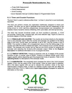
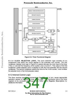
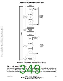
TIMER
EXTERNAL
INTERFACE
MODULE CONFIGURATION REGISTER
INTERRUPT REGISTER
CONTROL REGISTER
STATUS REGISTER
PRELOAD 1 REGISTER
TIN
I
M
B
(SYSTEM CLOCK)
CLOCK
CLOCK
TGATE
LOGIC
PRELOAD 2 REGISTER
SELECTED
CLOCK
COUNTER
CLOCK
16-BIT
COUNTER
MUX
MUX
8-BIT
PRESCALER
TOUT
TIMEOUT
COUNTER REGISTER
COMPARE REGISTER
16-BIT
COMPARATOR
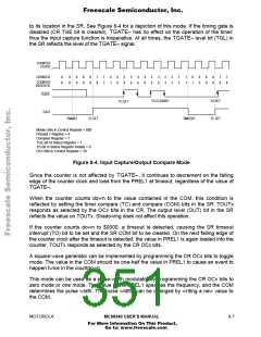
Figure 8-2. Timer Functional Diagram
8.1.1.4 CLOCK SELECTION LOGIC. The clock selection logic consists of two
multiplexers that select the clocks applied to the prescaler and counter. The first
multiplexer (labeled clock logic in Figure 8-2) selects between the clock input to the timer
(TINx) or one-half the frequency of the system clock (CLKOUT). This output of the first
multiplexer (called selected clock) is applied to both the 8-bit prescaler and the second
multiplexer. The second multiplexer selects the clock for the 16-bit counter, which is either
the selected clock or the 8-bit prescaler output.
8.1.2 Internal Control Logic
The timer receives operation commands on the IMB and, in turn, issues appropriate
operation signals to the internal timer control logic. This mechanism allows the timer
registers to be accessed and programmed. Refer to 8.4 Register Description for
additional information.
MOTOROLA
MC68340 USER’S MANUAL
8- 3
For More Information On This Product,
Go to: www.freescale.com

 FREESCALE [ Freescale ]