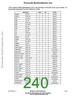
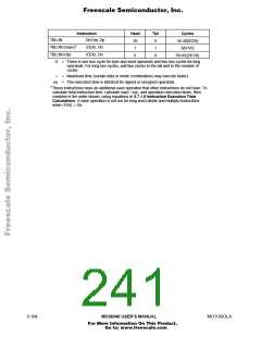
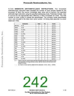
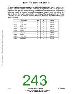
Freescale Semiconductor, Inc.
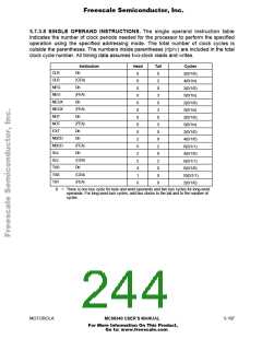
The numbers inside parentheses (r/p/w) are included in the total clock cycle number. All
timing data assumes two-clock reads and writes.
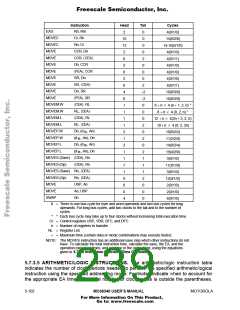
Instruction
Head
0
Tail
0
0
3
0
0
3
0
3
0
0
3
0
0
3
0
0
1
0
0
1
0
0
0
0
1
0
1
0
0
1
0
0
1
0
Cycles
2(0/1/0)
ADD(A)
ADD(A)
ADD
Rn, Rm
FEA , Rn
Dn, FEA
Dn, Dm
0
2(0/1/0)
0
5(0/1/x)
AND
0
2(0/1/0)
AND
FEA , Dn
Dn, FEA
Dn, Dm
0
2(0/1/0)
AND
0
5(0/1/x)
EOR
0
2(0/1/0)
EOR
Dn, FEA
Dn, Dm
0
5(0/1/x)
OR
0
2(0/1/0)
OR
FEA , Dn
Dn, FEA
Rn, Rm
0
2(0/1/0)
OR
0
5(0/1/x)
SUB(A)
SUB(A)
SUB
0
2(0/1/0)
FEA , Rn
Dn, FEA
Rn, Rm
0
2(0/1/0)
0
5(0/1/x)
CMP(A)
CMP(A)
CMP2 (Save)
CMP2 (Op)
MUL(su).W
0
2(0/1/0)
FEA , Rn
FEA , Rn
FEA , Rn
0
2(0/1/0)
*
1
3(0/1/0)
2
16-18(X/1/0)
26(0/1/0)
3(0/1/0)
FEA , Dn
0
*
MUL(su).L (Save)
MUL(su).L (Op)
MUL(su).L (Op)
DIVU.W
FEA , Dn
FEA , Dl
1
2
46-52(0/1/0)
46(0/1/0)
32(0/1/0)
42(0/1/0)
3(0/1/0)
FEA , Dn:Dl
FEA , Dn
FEA , Dn
FEA , Dn
FEA , Dn
FEA , Dn
FEA , Dn
Dn:Dm, Dp
CEA , Dn
CEA , Dn
Dn:Dm, Dp
CEA , Dn
CEA , Dn
2
0
DIVS.W
0
*
DIVU.L (Save)
1
DIVU.L (Op)
2
<46(0/1/0)
3(0/1/0)
*
DIVS.L (Save)
1
DIVS.L (Op)
TBL(su)
2
<62(0/1/0)
28-30(0/2/0)
3(0/1/0)
26
1
*
TBL(su) (Save)
TBL(su) (Op)
TBLSN
6
33-35(2X/1/0)
30-34(0/2/0)
3(0/1/0)
30
1
*
TBLSN (Save)
TBLSN (Op)
6
35-39(2X/1/0)
MOTOROLA
MC68340 USER’S MANUAL
5-103
For More Information On This Product,
Go to: www.freescale.com

 FREESCALE [ Freescale ]