Freescale Semiconductor, Inc.
Register Field:
In most commands, this field specifies the register number for operations performed on
an address or data register.
Extension Word(s) (as required):
At this time, no command requires an extension word to specify fully the operation to be
performed, but some commands require extension words for addresses or immediate
data. Addresses require two extension words because only absolute long addressing is
permitted. Immediate data can be either one or two words in length—byte and word
data each require a single extension word, long-word data requires two words. Both
operands and addresses are transferred most significant word first.
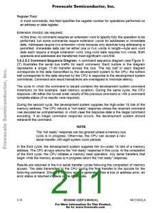
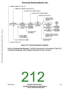
5.6.2.8.2 Command Sequence Diagram. A command sequence diagram (see Figure 5-
27) illustrates the serial bus traffic for each command. Each bubble in the diagram
represents a single 17-bit transfer across the bus. The top half in each diagram
corresponds to the data transmitted by the development system to the CPU; the bottom
half corresponds to the data returned by the CPU in response to the development system
commands. Command and result transactions are overlapped to minimize latency.
The cycle in which the command is issued contains the development system command
mnemonic (in this example, read memory location). During the same cycle, the CPU
responds with either the lowest order results of the previous command or with a command
complete status (if no results were required).
During the second cycle, the development system supplies the high-order 16 bits of the
memory address. The CPU returns a "not ready" response unless the received command
was decoded as unimplemented, in which case the response data is the illegal command
encoding. If an illegal command response occurs, the development system should
retransmit the command.
NOTE
The “not ready” response can be ignored unless a memory bus
cycle is in progress. Otherwise, the CPU can accept a new
serial transfer with eight system clock periods.
In the third cycle, the development system supplies the low-order 16 bits of a memory
address. The CPU always returns the “not ready” response in this cycle. At the completion
of the third cycle, the CPU initiates a memory read operation. Any serial transfers that
begin while the memory access is in progress return the “not ready” response.
Results are returned in the two serial transfer cycles following the completion of memory
access. The data transmitted to the CPU during the final transfer is the opcode for the
following command. Should a memory access generate either a bus or address error, an
error status is returned in place of the result data.
5- 74
MC68340 USER’S MANUAL
MOTOROLA
For More Information On This Product,
Go to: www.freescale.com

 FREESCALE [ Freescale ]