Freescale Semiconductor, Inc.
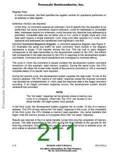
CPU
DEVELOPMENT SYSTEM
INSTRUCTION
REGISTER BUS
DATA
16
16
0
RCV DATA LATCH
COMMAND LATCH
DSI
SERIAL IN
PARALLEL OUT
PARALLEL IN
SERIAL OUT
DSO
SERIAL IN
PARALLEL OUT
PARALLEL IN
SERIAL OUT
16
STATUS
RESULT LATCH
EXECUTION
UNIT
16
STATUS
DATA
SYNCHRONIZE
MICROSEQUENCER
DSCLK
CONTROL
LOGIC
CONTROL
LOGIC
SERIAL
CLOCK
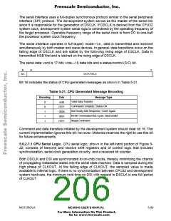
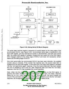
Figure 5-22. Debug Serial I/O Block Diagram
The serial state machine begins a sequence of events based on the rising edge of the
synchronized DSCLK (see Figure 5-23). Synchronized serial data is transferred to the
input shift register, and the received bit counter is decremented. One-half clock period
later, the output shift register is updated, bringing the next output bit to the DSO signal.
DSO changes relative to the rising edge of DSCLK and does not necessarily remain
stable until the falling edge of DSCLK.
One clock period after the synchronized DSCLK has been seen internally, the updated
counter value is checked. If the counter has reached zero, the receive data latch is
updated from the input shift register. At this same time, the output shift register is reloaded
with the “not ready/come again” response. Once the receive data latch has been loaded,
the CPU is released to act on the new data. Response data overwrites the “not ready”
response when the CPU has completed the current operation.
Data written into the output shift register appears immediately on the DSO signal. In
general, this action changes the state of the signal from a high (“not ready” response
status bit) to a low (valid data status bit) logic level. However, this level change only
occurs if the command completes successfully. Error conditions overwrite the “not ready”
response with the appropriate response that also has the status bit set.
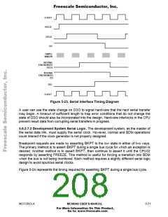
5- 70
MC68340 USER’S MANUAL
MOTOROLA
For More Information On This Product,
Go to: www.freescale.com

 FREESCALE [ Freescale ]