Freescale Semiconductor, Inc.
Development Support
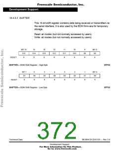
W/B — Word/Byte Transfer Flag
0 = Byte transfer
1 = Word transfer
BD/U — BDM Map/User Map Flag
Indicates whether BDM registers and ROM are mapped to addresses
$FF00 to $FFFF in the standard 64-Kbyte address space. Used only
by hardware read/write commands.
0 = BDM resources not in map
1 = BDM ROM and registers in map
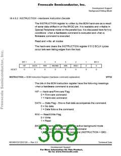
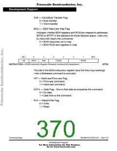
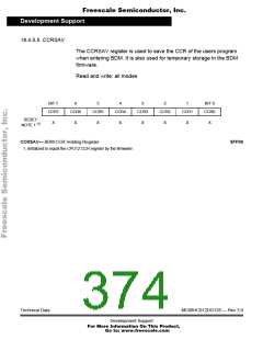
Bit 7
H/F
6
5
4
3
2
1
Bit 0
DATA
R/W
TTAGO
REGN
INSTRUCTION — BDM Instruction Register (firmware command bit explanation)
$FF00
The bits in the BDM instruction register have the following meanings
when a firmware command is executed.
H/F — Hardware/Firmware Flag
0 = Firmware command
1 = Hardware command
DATA — Data Flag - Shows that data accompanies the command.
0 = No data
1 = Data follows the command
R/W — Read/Write Flag
0 = Write
1 = Read
Technical Data
MC68HC912DG128 — Rev 3.0
Development Support
For More Information On This Product,
Go to: www.freescale.com

 FREESCALE [ Freescale ]