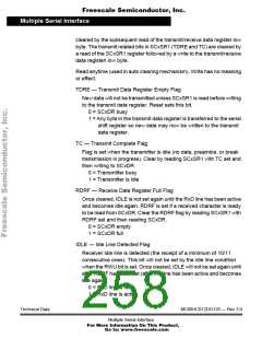
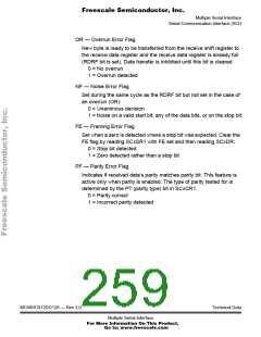
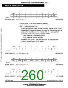
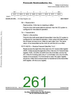
Freescale Semiconductor, Inc.
Multiple Serial Interface
14.5 Serial Peripheral Interface (SPI)
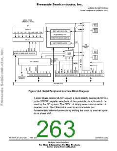
The serial peripheral interface allows the MC68HC912DG128 to
communicate synchronously with peripheral devices and other
microprocessors. The SPI system in the MC68HC912DG128 can
operate as a master or as a slave. The SPI is also capable of
interprocessor communications in a multiple master system.
When the SPI is enabled, all pins that are defined by the configuration
as inputs will be inputs regardless of the state of the DDRS bits for those
pins. All pins that are defined as SPI outputs will be outputs only if the
DDRS bits for those pins are set. Any SPI output whose corresponding
DDRS bit is cleared can be used as a general-purpose input.
A bidirectional serial pin is possible using the DDRS as the direction
control.
14.5.1 SPI Baud Rate Generation
The E Clock is input to a divider series and the resulting SPI clock rate
may be selected to be E divided by 2, 4, 8, 16, 32, 64, 128 or 256. Three
bits in the SP0BR register control the SPI clock rate. This baud rate
generator is activated only when SPI is in the master mode and serial
transfer is taking place. Otherwise this divider is disabled to save power.
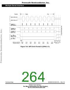
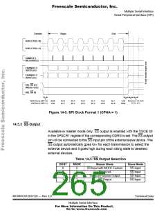
14.5.2 SPI Operation
In the SPI system the 8-bit data register in the master and the 8-bit data
register in the slave are linked to form a distributed 16-bit register. When
a data transfer operation is performed, this 16-bit register is serially
shifted eight bit positions by the SCK clock from the master so the data
is effectively exchanged between the master and the slave. Data written
to the SP0DR register of the master becomes the output data for the
slave and data read from the SP0DR register of the master after a
transfer operation is the input data from the slave.
Technical Data
MC68HC912DG128 — Rev 3.0
Multiple Serial Interface
For More Information On This Product,
Go to: www.freescale.com

 FREESCALE [ Freescale ]