Freescale Semiconductor, Inc.
Multiple Serial Interface
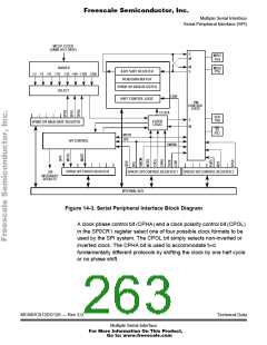
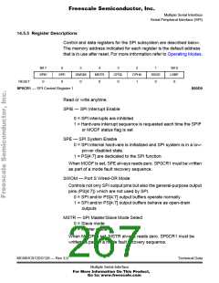
Serial Peripheral Interface (SPI)
Transfer
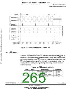
SCK (CPOL=0)
SCK (CPOL=1)
Begin
End
SAMPLE I
(MOSI/MISO)
e
r
s
CHANGE O
(MOSI pin)
CHANGE O
(MISO pin)
SEL SS (O)
(Master only)
SEL SS (I)
tL
MSB first (LSBF=0): MSB
LSB first (LSBF=1):
LSB
tT
LSB Minimum 1/2 SCK
for tT, tl, tL
tI
tL
Bit 6
Bit 1
Bit 5
Bit 2
Bit 4
Bit 3
Bit 3
Bit 4
Bit 2
Bit 5
Bit 1
Bit 6
MSB
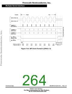
Figure 14-5. SPI Clock Format 1 (CPHA = 1)
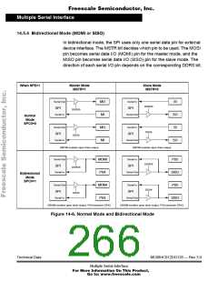
14.5.3 SS Output
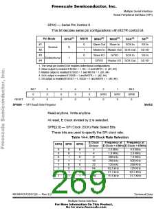
Available in master mode only, SS output is enabled with the SSOE bit
in the SP0CR1 register if the corresponding DDRS is set. The SS output
pin will be connected to the SS input pin of the external slave device. The
SS output automatically goes low for each transmission to select the
external device and it goes high during each idling state to deselect
external devices.
Table 14-3. SS Output Selection
DDS7
SSOE
Master Mode
SS Input with MODF Feature
Reserved
Slave Mode
SS Input
SS Input
SS Input
SS Input
0
0
1
1
0
1
0
1
General-Purpose Output
SS Output
MC68HC912DG128 — Rev 3.0
Technical Data
Multiple Serial Interface
For More Information On This Product,
Go to: www.freescale.com

 FREESCALE [ Freescale ]