Freescale Semiconductor, Inc.
Enhanced Capture Timer
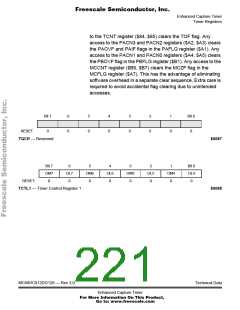
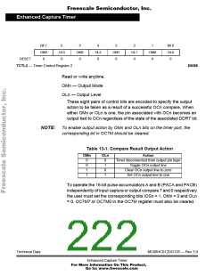
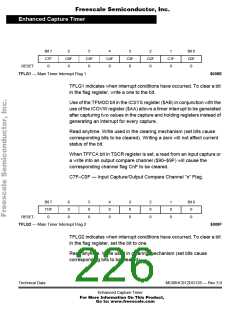
Bit 7
OM3
0
6
OL3
0
5
OM2
0
4
OL2
0
3
OM1
0
2
OL1
0
1
OM0
0
Bit 0
OL0
0
RESET:
TCTL2 — Timer Control Register 2
$0089
Read or write anytime.
OMn — Output Mode
OLn — Output Level
These eight pairs of control bits are encoded to specify the output
action to be taken as a result of a successful OCn compare. When
either OMn or OLn is one, the pin associated with OCn becomes an
output tied to OCn regardless of the state of the associated DDRT bit.
NOTE: To enable output action by OMn and OLn bits on the timer port, the
corresponding bit in OC7M should be cleared.
Table 13-1. Compare Result Output Action
OMn
OLn
Action
0
0
1
1
0
1
0
1
Timer disconnected from output pin logic
Toggle OCn output line
Clear OCn output line to zero
Set OCn output line to one
To operate the 16-bit pulse accumulators A and B (PACA and PACB)
independently of input capture or output compare 7 and 0 respectively
the user must set the corresponding bits IOSn = 1, OMn = 0 and OLn
= 0. OC7M7 or OC7M0 in the OC7M register must also be cleared.
Technical Data
MC68HC912DG128 — Rev 3.0
Enhanced Capture Timer
For More Information On This Product,
Go to: www.freescale.com

 FREESCALE [ Freescale ]