Freescale Semiconductor, Inc.
Clock Functions
Clock Function Registers
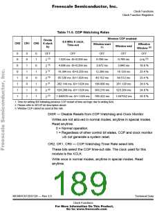
Table 11-5. COP Watchdog Rates
Window COP enabled:
Divide
CR2 CR1 CR0 X clock
by
8.0 MHz X clock.
Time-out
Window start
Effective
Window (2)
Window end
(1)
0
0
0
0
1
1
1
1
0
0
1
1
0
0
1
1
0
1
0
1
0
1
0
1
OFF
2 13
2 15
2 17
2 19
2 21
2 22
2 23
OFF
OFF
OFF
OFF
0 % (3)
18.8 %
23.4 %
23.4 %
24.6 %
24.8 %
24.9 %
1.024 ms -0/+0.256 ms
4.096 ms -0/+0.256 ms
16.384 ms -0/+0.256 ms
65.536 ms -0/+1.024 ms
262.144 ms -0/+1.024 ms
524.288 ms -0/+1.024 ms
1.048576 ms -0/+1.024 ms
0.768 ms
0.768 ms
3.072 ms
3.840 ms
12.288 ms
49.152 ms
196.608 ms
393.216 ms
786.432 ms
16.128 ms
64.512 ms
261.120 ms
523.264 ms
1.047552 ms
1. Time for writing $55 following previous COP restart of time-out logic due to writing $AA.
2. Please refer to WCOP bit description above.
3. Window COP cannot be used at this rate.
DISR — Disable Resets from COP Watchdog and Clock Monitor
Writes are not allowed in normal modes, anytime in special modes.
Read anytime.
0 = Normal operation.
1 = Regardless of other control bit states, COP and clock monitor
will not generate a system reset.
CR2, CR1, CR0 — COP Watchdog Timer Rate select bits
These bits select the COP time-out rate. The clock used for this
module is the XCLK.
Write once in normal modes, anytime in special modes. Read
anytime.
MC68HC912DG128 — Rev 3.0
Technical Data
Clock Functions
For More Information On This Product,
Go to: www.freescale.com

 FREESCALE [ Freescale ]