Table of Contents
Part 1: Overview . . . . . . . . . . . . . . . . . . . . . . .5
Part 8: General Purpose Input/Output (GPIO)
1.1. 56F8367/56F8167 Features . . . . . . . . . . . . . 5
1.2. Device Description . . . . . . . . . . . . . . . . . . . . 7
1.3. Award-Winning Development Environment . 9
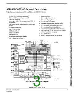
1.4. Architecture Block Diagram . . . . . . . . . . . . 10
1.5. Product Documentation . . . . . . . . . . . . . . . 14
1.6. Data Sheet Conventions . . . . . . . . . . . . . . . 14
. . . . . . . . . . . . . . . . . . . . . . . . . . . . . . . . . . . 132
8.1. Introduction . . . . . . . . . . . . . . . . . . . . . . . .132
8.2. Memory Maps . . . . . . . . . . . . . . . . . . . . . . 132
8.3. Configuration . . . . . . . . . . . . . . . . . . . . . . .133
Part 9: Joint Test Action Group (JTAG) . 137
9.1. 56F8367 Information. . . . . . . . . . . . . . . . . 137
Part 2: Signal/Connection Descriptions . . .15
2.1. Introduction . . . . . . . . . . . . . . . . . . . . . . . . . 15
2.2. Signal Pins . . . . . . . . . . . . . . . . . . . . . . . . . 18
Part 10: Specifications . . . . . . . . . . . . . . . 138
10.1. General Characteristics. . . . . . . . . . . . . . 138
10.2. DC Electrical Characteristics . . . . . . . . . .142
10.3. AC Electrical Characteristics . . . . . . . . . .146
10.4. Flash Memory Characteristics . . . . . . . . .147
10.5. External Clock Operation Timing . . . . . . .147
10.6. Phase Locked Loop Timing. . . . . . . . . . . 148
10.7. Crystal Oscillator Timing . . . . . . . . . . . . .148
10.8. External Memory Interface Timing . . . . . .149
10.9. Reset, Stop, Wait, Mode Select, and
Part 3: On-Chip Clock Synthesis (OCCS) . .39
3.1. Introduction . . . . . . . . . . . . . . . . . . . . . . . . . 39
3.2. External Clock Operation . . . . . . . . . . . . . . 39
3.3. Registers . . . . . . . . . . . . . . . . . . . . . . . . . . 41
Part 4: Memory Operating Modes (MEM) . .41
4.1. Introduction . . . . . . . . . . . . . . . . . . . . . . . . . 41
4.2. Program Map . . . . . . . . . . . . . . . . . . . . . . . 42
4.3. Interrupt Vector Table . . . . . . . . . . . . . . . . . 43
4.4. Data Map . . . . . . . . . . . . . . . . . . . . . . . . . . 47
4.5. Flash Memory Map . . . . . . . . . . . . . . . . . . . 47
4.6. EOnCE Memory Map . . . . . . . . . . . . . . . . . 49
4.7. Peripheral Memory Mapped Registers . . . . 49
4.8. Factory Programmed Memory . . . . . . . . . . 80
Interrupt Timing . . . . . . . . . . . . . .151
10.10. Serial Peripheral Interface (SPI) Timing . . . .
. . . . . . . . . . . . . . . . . . . . . . . . . . .154
10.11. Quad Timer Timing . . . . . . . . . . . . . . . .157
10.12. Quadrature Decoder Timing . . . . . . . . . .157
10.13. Serial Communication Interface (SCI)
Timing . . . . . . . . . . . . . . . . . . . . .158
10.14. Controller Area Network (CAN) Timing .159
10.15. JTAG Timing . . . . . . . . . . . . . . . . . . . . .159
10.16. Analog-to-Digital Converter (ADC)
Parameters. . . . . . . . . . . . . . . . . 161
10.17. Equivalent Circuit for ADC Inputs . . . . . .164
10.18. Power Consumption . . . . . . . . . . . . . . . .164
Part 5: Interrupt Controller (ITCN) . . . . . . . .81
5.1. Introduction . . . . . . . . . . . . . . . . . . . . . . . . . 81
5.2. Features . . . . . . . . . . . . . . . . . . . . . . . . . . . 81
5.3. Functional Description. . . . . . . . . . . . . . . . . 81
5.4. Block Diagram. . . . . . . . . . . . . . . . . . . . . . . 83
5.5. Operating Modes. . . . . . . . . . . . . . . . . . . . . 83
5.6. Register Descriptions . . . . . . . . . . . . . . . . . 84
5.7. Resets . . . . . . . . . . . . . . . . . . . . . . . . . . . . 110
Part 11: Packaging . . . . . . . . . . . . . . . . . . 166
11.1. 56F8367 Package and Pin-Out
Information . . . . . . . . . . . . . . . . . .166
11.2. 56F8167 Package and Pin-Out
Part 6: System Integration Module (SIM) .111
6.1. Overview . . . . . . . . . . . . . . . . . . . . . . . . . 111
6.2. Features . . . . . . . . . . . . . . . . . . . . . . . . . . 111
6.3. Operating Modes. . . . . . . . . . . . . . . . . . . . 112
6.4. Operating Mode Register . . . . . . . . . . . . . 112
6.5. Register Descriptions . . . . . . . . . . . . . . . . 113
6.6. Clock Generation Overview . . . . . . . . . . . 127
6.7. Power Down Modes Overview . . . . . . . . . 128
6.8. Stop and Wait Mode Disable Function . . . 128
6.9. Resets . . . . . . . . . . . . . . . . . . . . . . . . . . . 129
Information . . . . . . . . . . . . . . . . . .173
Part 12: Design Considerations . . . . . . . . 177
12.1. Thermal Design Considerations . . . . . . . .177
12.2. Electrical Design Considerations . . . . . . .178
12.3. Power Distribution and I/O Ring
Implementation . . . . . . . . . . . . . .179
Part 13: Ordering Information . . . . . . . . . 180
Part 7: Security Features . . . . . . . . . . . . . .129
7.1. Operation with Security Enabled . . . . . . . 129
7.2. Flash Access Blocking Mechanisms . . . . 130
56F8367 Technical Data, Rev. 9
4
Freescale Semiconductor
Preliminary

 FREESCALE [ Freescale ]