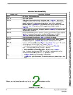
Document Revision History
Version History
Description of Change
Pre-release, Alpha customers only
Initial Public Release
Rev 0
Rev 1.0
Rev 2.0
Added output voltage maximum value and note to clarify in Table 10-1.; also removed
overall life expectancy note, since life expectancy is dependent on customer usage and
must be determined by reliability engineering. Clarified value and unit measure for
Maximum allowed PD in Table 10-3. Corrected note about average value for Flash Data
Retention in Table 10-4. Added new RoHS-compliant orderable part numbers in
Table 13-1.
Rev 3.0
Rev 4.0
Added 160MAPBGA information, TA equation updated in Table 10-4 and additional minor
edits throughout data sheet
Deleted formula for Max Ambient Operating Temperature (Automotive) and Max Ambient
Operating Temperature (Industrial) and corrected Flash Endurance to 10,000 in
Table 10-4. Added RoHS-compliance and “pb-free” language to back cover.
Rev 5.0
Rev 6.0
Correcting MBGA pin assignments in Table 2-2 for MOSI0 and MISO0
Added information/corrected state during reset in Table 2-2. Clarified external reference
crystal frequency for PLL in Table 10-14 by increasing maximum value to 8.4MHz.
Rev 7.0
Rev. 8
Corrected CLKO and HOME1 labels in Figure 11-2 and Table 11-2; replaced “Tri-stated”
with an explanation in State During Reset column in Table 2-2.
• Added the following note to the description of the TMS signal in Table 2-2:
Note: Always tie the TMS pin to VDD through a 2.2K resistor.
• Added the following note to the description of the TRST signal in Table 2-2:
Note: For normal operation, connect TRST directly to VSS. If the design is to be used in a
debugging environment, TRST may be tied to VSS through a 1K resistor.
• Add Figure 10-1 showing current voltage characteristics.
Rev. 9
• In Table 10-24, correct interpretation of Calibration Factors to be viewed as worst case
factors.
Please see http://www.freescale.com for the most current data sheet revision.
56F8367 Technical Data, Rev. 9
2
Freescale Semiconductor
Preliminary

 FREESCALE [ Freescale ]