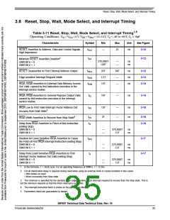
Reset, Stop, Wait, Mode Select, and Interrupt Timing
3.6 Reset, Stop, Wait, Mode Select, and Interrupt Timing
1,5
Table 3-11 Reset, Stop, Wait, Mode Select, and Interrupt Timing
Operating Conditions: VSS = VSSA = 0 V, VDD = VDDA = 3.0–3.6 V, TA = –40° to +85°C, CL ≤ 50pF
Characteristic
Symbol
Min
Max
Unit
See Figure
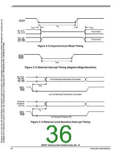
3-12
RESET Assertion to Address, Data and Control Signals
High Impedance
tRAZ
—
21
ns
Minimum RESET Assertion Duration2
OMR Bit 6 = 0
OMR Bit 6 = 1
tRA
3-12
275,000T
128T
—
—
ns
ns
RESET Deassertion to First External Address Output
Edge-sensitive Interrupt Request Width
tRDA
tIRW
tIDM
33T
1.5T
15T
34T
—
ns
ns
ns
3-12
3-13
3-14
IRQA, IRQB Assertion to External Data Memory Access
Out Valid, caused by first instruction execution in the
interrupt service routine
—
IRQA, IRQB Assertion to General Purpose Output Valid,
caused by first instruction execution in the interrupt
service routine
tIG
16T
—
ns
3-14
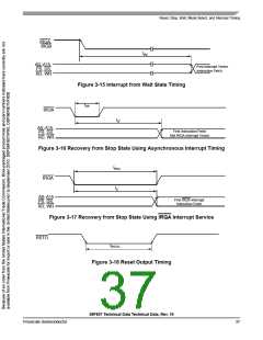
3-15
IRQA Low to First Valid Interrupt Vector Address Out
recovery from Wait State3
tIRI
13T
2T
—
—
ns
ns
IRQA Width Assertion to Recover from Stop State4
tIW
tIF
3-16
3-16
Delay from IRQA Assertion to Fetch of first instruction
(exiting Stop)
OMR Bit 6 = 0
OMR Bit 6 = 1
—
—
275,000T
12T
ns
ns
Duration for Level Sensitive IRQA Assertion to Cause
the Fetch of First IRQA Interrupt Instruction (exiting Stop)
OMR Bit 6 = 0
tIRQ
3-17
3-17
—
—
275,000T
12T
ns
ns
OMR Bit 6 = 1
Delay from Level Sensitive IRQA Assertion to First
Interrupt Vector Address Out Valid (exiting Stop)
OMR Bit 6 = 0
tII
—
—
275,000T
12T
ns
ns
OMR Bit 6 = 1
1. In the formulas, T = clock cycle. For an operating frequency of 80MHz, T = 12.5ns.
2. Circuit stabilization delay is required during reset when using an external clock or crystal oscillator in two cases:
• After power-on reset
• When recovering from Stop state
3. The minimum is specified for the duration of an edge-sensitive IRQA interrupt required to recover from the Stop state. This is
not the minimum required so that the IRQA interrupt is accepted.
4. The interrupt instruction fetch is visible on the pins only in Mode 3.
5. Parameters listed are guaranteed by design.
56F807 Technical Data Technical Data, Rev. 16
Freescale Semiconductor
35

 FREESCALE [ Freescale ]